LED thinner than hair developed using tungsten diselenide
Scientists at University of Washington have built 3 atom thin LED made from atom-scale sheets of the molecular semiconductor material tungsten diselenide, a thinnest-known compound semiconductor material. Researchers use adhesive tape to extract a single sheet of this material from thick, layered pieces, a method similar to isolating one-atom-thick flakes graphene from graphite.
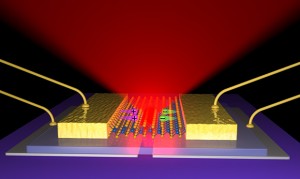
The above picture is the graphical representation of how layers of the 2-D LED emitting light. “We are able to make the thinnest-possible LEDs, only three atoms thick yet mechanically strong. Such thin and foldable LEDs are critical for future portable and integrated electronic devices,” said Xiaodong Xu, a UW assistant professor in materials science and engineering and in physics. The paper written bv Xu, Jason Ross, a UW materials science and engineering graduate student has appeared online March 9 in Nature Nanotechnology. “These are 10,000 times smaller than the thickness of a human hair, yet the light they emit can be seen by standard measurement equipment,” Ross said. “This is a huge leap of miniaturization of technology, and because it’s a semiconductor, you can do almost everything with it that is possible with existing, three-dimensional silicon technologies,” Ross said. ...
The above picture is the graphical representation of how layers of the 2-D LED emitting light. “We are able to make the thinnest-possible LEDs, only three atoms thick yet mechanically strong. Such thin and foldable LEDs are critical for future portable and integrated electronic devices,” said Xiaodong Xu, a UW assistant professor in materials science and engineering and in physics. The paper written bv Xu, Jason Ross, a UW materials science and engineering graduate student has appeared online March 9 in Nature Nanotechnology. “These are 10,000 times smaller than the thickness of a human hair, yet the light they emit can be seen by standard measurement equipment,” Ross said. “This is a huge leap of miniaturization of technology, and because it’s a semiconductor, you can do almost everything with it that is possible with existing, three-dimensional silicon technologies,” Ross said. ...
You've read this far — sign in to keep reading