TO-Leadless package from Infineon offers electrical performance and size advantage
Infineon has introduced the new TO-Leadless package for its power semiconductor devices in the current range of 300 Amperes. TO-Leadless package offers less package resistance and smaller size and also improved EMI behavior. The OptiMOS MOSFET available in this package is suggested for applications with high power and reliability requirements such as forklift, light electric vehicles, eFuse, PoL (Point of Load) and telecom systems.
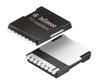
TO-Leadless offers 60 percent smaller package size compared to D 2PAK. The 50 percent reduced height make is suitable for applications where the device thickness matters. Low package parasitic inductances result in an improved EMI behavior. “With TO-Leadless Infineon is the first semiconductor company introducing a 0.75mΩ 60V MOSFET. This reduces the number of parallel MOSFETs in a forklift application and increases power density“, said Richard Kuncic, Senior Director Low Voltage Power Conversion at Infineon Technologies. “This package offers our customers significant advantages for high power applications where highest levels of efficiency and reliability are desired.” In addition, TO-Leadless comes with a 50 percent bigger solder contact area which leads to lower current density. This helps to avoid electro migration at...
TO-Leadless offers 60 percent smaller package size compared to D 2PAK. The 50 percent reduced height make is suitable for applications where the device thickness matters. Low package parasitic inductances result in an improved EMI behavior. “With TO-Leadless Infineon is the first semiconductor company introducing a 0.75mΩ 60V MOSFET. This reduces the number of parallel MOSFETs in a forklift application and increases power density“, said Richard Kuncic, Senior Director Low Voltage Power Conversion at Infineon Technologies. “This package offers our customers significant advantages for high power applications where highest levels of efficiency and reliability are desired.” In addition, TO-Leadless comes with a 50 percent bigger solder contact area which leads to lower current density. This helps to avoid electro migration at...
You've read this far — sign in to keep reading