Copper Interconnects at the Breaking Point: Why They Are Failing in Sub-3 nm AI Chips
As artificial intelligence (AI) accelerators push toward 2 nm and below, the industry’s decades-long reliance on copper (Cu) interconnects in the back-end-of-line (BEOL) is facing fundamental physical limits. Gate-All-Around (GAA) nanosheet transistors—adopted by TSMC (N2), Intel (18A/20A), and Samsung (SF2) deliver superior electrostatic control and power efficiency. Yet the dense, high-current interconnect networks required for massive parallelism in AI workloads expose copper’s scaling weaknesses: exploding resistivity, self-heating, thermo-mechanical stress, and reliability degradation. These issues are no longer incremental; they threaten the performance-per-watt gains essential for next-generation AI training and inference chips.
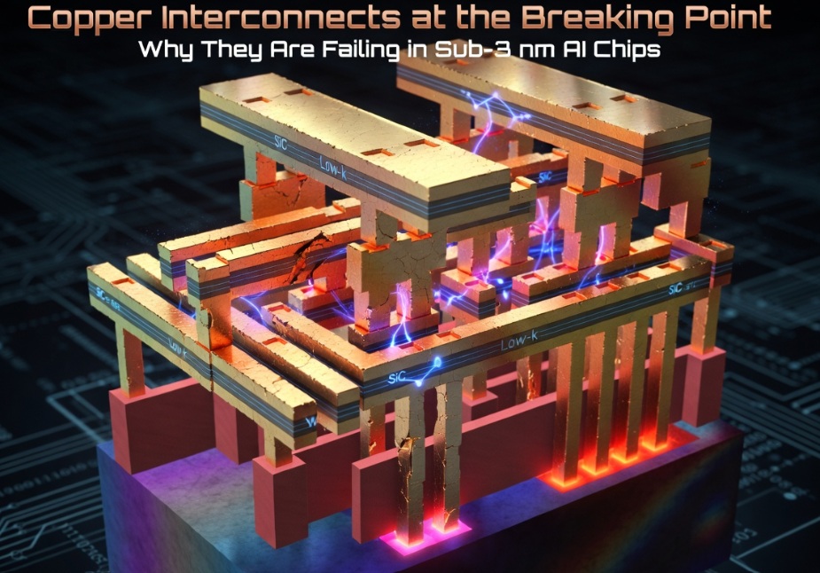
The Resistivity Wall: Electron Scattering Takes Over: At metal pitches below ~20–25 nm (typical for sub-3 nm nodes), copper’s effective resistivity rises dramatically often 5–10× higher than bulk values due to surface and grain-boundary scattering. The mean free path of electrons in Cu (~40 nm) exceeds the wire dimensions, leaving little room for the conductor after TaN barriers, Co liners, and caps consume 30–50 % of the cross-section.
Result: RC...