India Electronics and Semiconductor roundup via IESA vision Summit 2024: Cheetahs are bred
Date: 13/03/2024
EEHerald being operated from Bangalore, we have nearly covered all the IESA Vision Summits held since 2009 except the one during Covid. We already wrote two short articles after attending IESA VS 2024 giving the overall observations (You can find links to those articles at the end of this article). While broad Indian semiconductor eco is under construction all over India with the government, industry and academia all playing their roles. These stakeholders could meet and share experiences, trends, and their innovations to the attendees at the event. It was like two-day run on what all happened in 2023 and whats to look forward in 2024. Here in this article, I go little in detail with key points made by some of the speakers and panelists.
AI chips: Sid Sheth, Founder & CEO, d-Matrix presented his keynote titled "India's Role in the Global Explosion of Generative AI on AI chips".
Sid Sheth started how generative AI tools such as ChatGPT creating great excitement and gripping the whole world. His company d-Matrix is trying to solve the next-gen computing problem that will allow generative AI to be commercially viable for everyone. He finds it encouraging to see Indian government under the leadership of Prime Minister Narendra Modi embracing AI as kinetic enabler for achieving a $1 billion digital economy. Generative AI has the potential to add 1.5 trillion to Indian GDP by 2030, a staggering amount of productivity gain that can be made available by AI. He also explained how Indias AI project Bhashini, helping to break down the language barriers of India. Bhashini to help more Indian langauge content available on the Internet. BHASHINI is democratizing AI. D-Matrix is focused on inference and deployment part of AI where it help efficiently deploy these models.
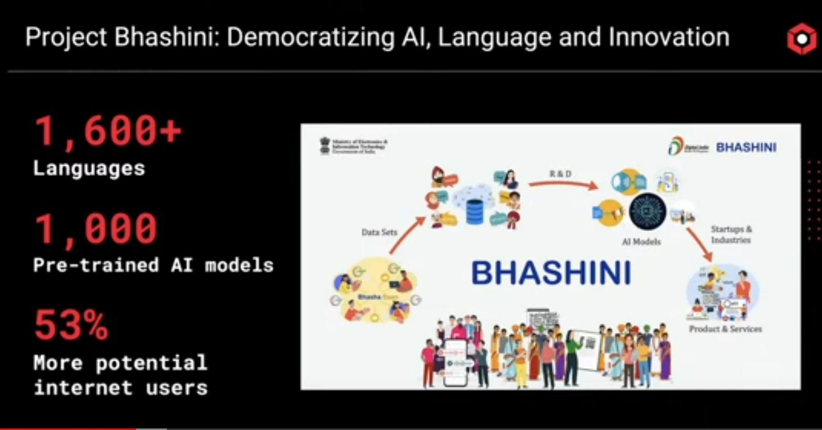
Pic: One of the slide on BHASHINI
Here are the other points from his keynote:
AI servers running chatGPT need thousands of GPUs which are very costly. GPUs are built 30 year ago and they are not the most efficient processors to run chatGPT like applications. They consume lot of power. He shared a dirty secret in the generative AI race. Integrating LLMs into search engines could mean a fivefold increase in computing power and huge carbon emissions. Without sustainable practices, AI will consume more energy than the human workforce by 2025. The energy needed to power AI could account for up to 3.5% of global electricity consumption by 2030 if current practices remain unchanged, calling it a unsustainable trajectory. The other challenge is size of AI model, the models are getting larger as time goes, that means they requires lot more compute and costs lot more.
He said We are on a trajectory that if we don't do something differently or change the trajectory, we will be spending more than the entire US GDP to run the AI computing by 2030. d-Matrix is trying to solve this problem by coming out with a fundamentally new computing paradigms called digital in-memory computing, this breaks through the AI barrier. Today's AI barrier is between compute and memory where data need to be fetched from the memory and used by the compute in repetitive and parallel fashion and send back to the memory consuming lot of energy and time. Traditional architectures such as CPUs, GPUs and FPGAs use an architecture called Von Neumann architecture which doesn't address AI barrier issue. D-Matrix has come out with a solution which breaks through this barrier by using a concept called in-memory computing.
d-Matrix has developed a generation of silicon chips based on its in-memory computing. These chips are named as Nighthawk, JayhawkI and JayhawkII. They have built chips on 6 nm nodes and used chiplets. They are offering both enterprise grade software and purpose built hardware for building generative AI models where they are launching a first product called Corsair. I could see the demo at it's stall in the event and the performance was impressive and in fact better than GPUs.
Chiplets:
The 2nd keynote titled "Symphony: India, Semiconductors, AI & Chiplets" was from Mohit Gupta SVP & GM, Custom Silicon & IP, Alphawave Semi.
Mohit touched upon the global semiconductor market opportunity. He shared market research estimate data from McKinsey, where the semiconductor market to reach US$ 1 Trillion+ by 2030, where data-centres, automotive and wireless to have a share of 70%. He explained the economics of Chiplets in the AI era semiconductor market. The cost of AI SOC can come down by 50% of even more, if it is a heterogeneous SoC with chiplets compared to monolithic advanced node SoC chip for the same kind of application. The low yield for a large die-size monolithic 3nm chip costs huge. IC design and package optimizations are the future of advancing compute semiconductors, according to him.
Alphawave has big operations in India, where most part of its chiplet design is done. They have a goal of increasing their staff strength in India to one thousand by 2030.
IDM semiconductor business prospective:
Lars Reger, EVP & CTO, NXP Semiconductor started by displaying a old but relevant slide of global megatrends driving the industry. They are resilient and efficient factories buildings, seamless interaction and anticipation, increased security threats and need for safety, always connected and sensing, demographic change, climate change, limitations of resources, supply continuity, infrastructure upgrades, and artificial intelligence. Increased automation is helping to address these trends with most advanced automation solution called digital twin, according to him. He shared some of the market forecast figures such as 50 billion smart connected devices by 2030, AI semiconductor revenue reaching $75 billion 2025, 5G to cover 60% of the world, 50% of automotive to be electrified and have level2 advanced driver assistance systems by 2030. He also explained how today's advanced car think like human brain. Smart homes is another big market he highlighted where he shared by 2027 more than 2 billion smart home connected devices will be shipped annually.
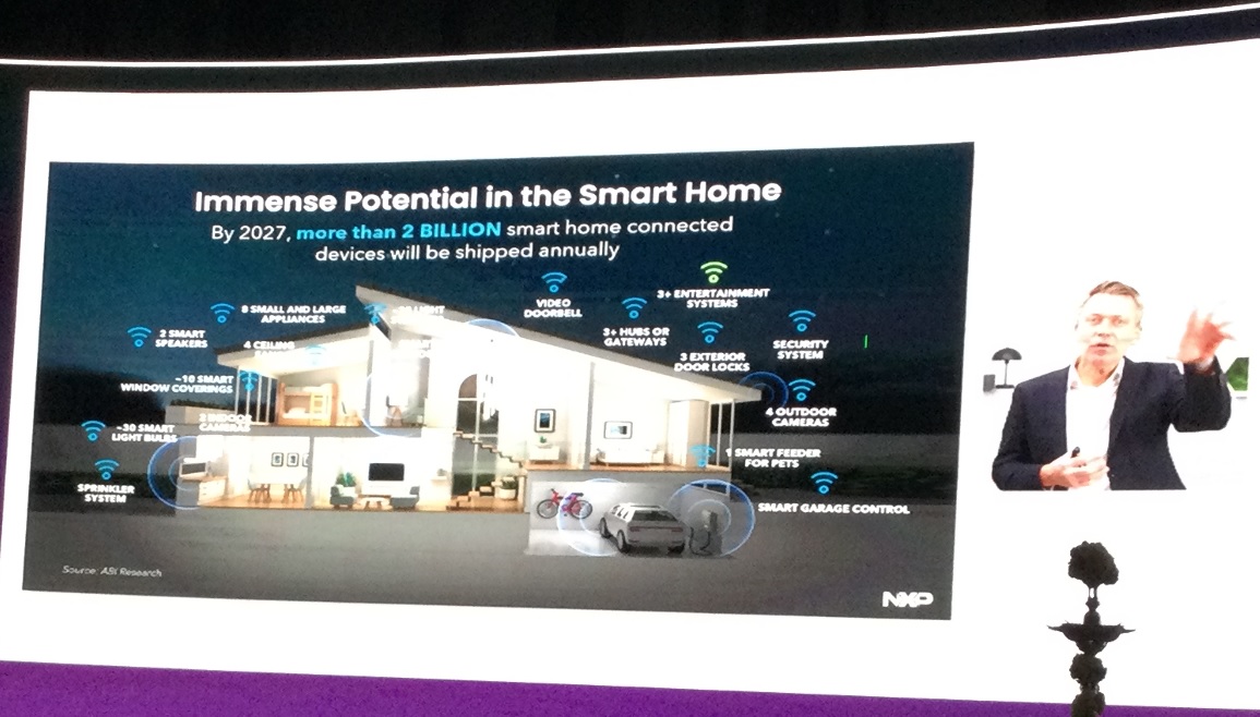
Pic: Lars Regar slide on smarthome opportunity
At this year's event the panel discussions were more interesting than keynotes. Panel discussions covered India electronics and semiconductor design, manufacturing, supply chain, and verticals such as AI and automotive.Here are some of the highlights I would like share from panel discussions:
Panel: Development on the ground: electronics and semiconductor manufacturing, semiconductor packaging.
This session was moderated by Ravi Bhatkal, Managing Director McDermid Alpha India. The panelists include Amrit Manwani CMD Sahasra semiconductor, Satendra Singh CEO Syrma SGS, Deepak Chadha, Kaynes Technology and Dr. Andie Mackie, Principal Engineer for advanced material, Indium Corp.
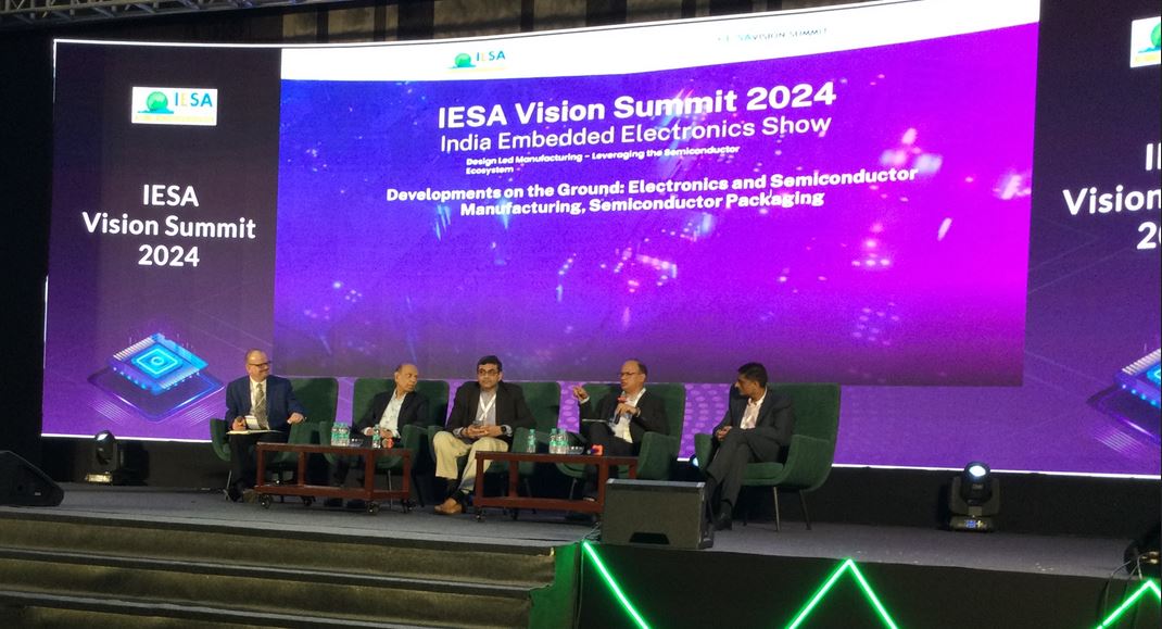
Pic: Above said panel
Amrit Manwani explained 5 key issues of manpower-shortage, raw-material shortage, lack of chip foundry, semiconductor packaging equipment availability, and equipment servicing faced by semiconductor packaging as well as for advanced PCB making. He suggested the triveni sangam of government, industry and academia can do wonders for these challenges by working as a single entity and to create robust ecosystem and look at global opportunities rather than look at India alone.
Satendra Singh opines that point of inflection will be when once India's per-capita income reaches $3000 . He said That's where you start going up significantly. That point is around the corner for us. Business is not only for global companies but also for local companies. We have to make sure that this business is ours. To improve the quality of engineering education he suggested its time for India to say that nobody can get a degree unless you complete 6 to 12 months of training in industry. Millions of engineers we have and every year come out have pretty capable. This is like glass half full. We have the basic ingredients, we have to orient them more practical from theoretical orientation says Satendra.
He said "If you want manufacturing to be sticky and sustainable, and which will not evaporate after a change in the policy, such as some changes in the global geopolitics. Then we need to have design supply chain and manufacturing all three working together. Electronic manufacturing companies need to focus more on ODM rather than EMS. That is design plus manufacturing."
Deepak said "We can definitely say India is on right track in terms of contributing to manufacturing and electronics segment as well." He alerts to become electronic nation just doing PCB assembly will not help government or companies, we need to scale up.
Andy explained latest trends in OSAT, where chip foundries playing bigger role in advanced packaging such as hybrid bonding. He suggested flipchip and wirebonding is for OSAT and it's kind of an easy button.
Panel: India's startup ecosystem, uniqueness, way forward to sustainable innovation: Brand building through product creation and innovation.
The panel moderated by Nishit Gupta, Scientist E MeitY and the panelists include Gautam Singh Founder and CEO Fermionic Design, Neel Gala CTO and Co-founder Incore Semiconductor, Anil Kempanna CEO Cientra, Uttam Singhal EVP and MD Signoff Semiconductor and Subodh Sachan STPI.
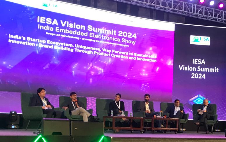
Pic: Above said panel
Neel heads a RISC-V based CPU design company where they have developed CPUs for range of application and they also provide services in developing RISC V based chips. Neel started off saying "Abhi Jugaad Nahi Chalega". He point out semiconductor is not a local market because of its scale and volumes. None of that will work if just serving the local market. He suggests people need to lobby selling the problem first then sell the solution in the semiconductor space.
Gautam, who is working in the niche requirement of defence sector highlighted the defence market requirements. Some of his points include:
1.Semiconductor role is important in defence sector it helps in defence sector to be self-reliant
2. Adoption of innovation in defence sector is one of the highest from the product or system point of view. It is touching all the domains of semiconductor such as communication, power management, etc.
3. The reliability requirements of aerospace and defence is supreme, much more higher than commercial or industrial, you don't want life of your device 18/24 months, it need to operate for 15 to 20 years.
Uttam said "In 2022 Indian semiconductor market was US$ 27 to 28 billion the growth rate projected was about 11%, so by 2030 reaching close to 70 to 80 billion US dollars. To achieve this growth rate we need catalysts, we need support, we need extra things to make it sustainable. Signoff was fortunate to get Karnataka government's ESDM grants for about two years that really helped us to do lot of in-house development."
Signoff is a big-time advocates of RISC V, where they have developed in-house embedded solutions called KAVERI.
Uttam ended by saying "We are headquartered in India, we are expanding our organization across the globe. We do have an office in China if required who knows we will expand in China."
Anil left Intel before he joined Cientra. He explained how he came across set of challenges very unique to semiconductor product startup. He said "semiconductor startup is not like fin-tech start-up where they invest two crores and they get 20 crores in three years. In semicon startups, for invest of US$ 1 million we hardly get a MCU (to design an own MCU chip)."
He further said "To do (design) a mid-size SOC you need US$20 to 30 million, how do you do that, I came across this company called Cientra, they started with the services based company. I found Ips, solutions, patents and some software products, I found it unique. Here is a company enabling chip companies to create products. I found it unique be the enabler of how to create a semiconductor product companies." Cientra is exactly doing that now enabling design of chips.
He further said "We have delivered a reference designs with some of our partners. We are providing Ips. We are transforming from the attitude of service semiconductor start-ups to become not exactly products but product enabling startups"
"The Rome is not something be built in a day let's not wait Rome to be built-in years, lets that happen in a few years from now." is Anil's final quote.
STPI is doing a great job by implementing many schemes in tier 2 cities. The scheme which creates difference in last four/five years. Subodh said "Extending the government mission of advancing the government vision of start-up entrepreneurship ecosystem. It was done for economic development, innovation led products creation and also for job creation prospective."
My views:
Since India started making semiconductor chips back in 1980s, there is always a program from the government of India to grow semiconductor industry in India. But there were some shortcomings in the form of allotted resources, strategies, timing and extra-sharp-focus on a fast moving target to make ourselves globally competitive compared to far-east geographies, if not western world.
We were late to realize semiconductor industry is a very fast moving target. Possibly some errors in execution as well. In semiconductors few weak point can kill the whole effort. In that sense, we should fully appreciate all the previous attempts at building semiconductor manufacturing base in India.
We can compare our strategy to Indian Railways, comparatively safe, reliable and very large rail network, but no speedy trains, and lack of cleanlines. Off-course, now we have Vande-Bharat. We are changing. One important point though is lot of effort poured since decades is not going wasted, today's generation can rely on that platform to compete in tomorrows world. If we had not had that legacy of reliable, safe and large rail network, we could not be able to build Vande Bharats of today.
Somehow the spirit to compete was not lost although severely lagging behind our own combined capabilities. Now the government is giving exponential push but still with shortcoming which are not in India's control such as ability to build advanced fabs in Angstrom nodes for making AI chips and make such chip with our own machine tools/equipments. But people in this game know how tough it is, they may end up loosing hope. But India need to latch-on with its goal of becoming global semiconductor hub. India needs to device its own strategy to survive and grow its electronics technology driven systems amid geo-political disruptions of both of man-made and nature-created such as Covid and any such disruptions. With the cabinet approval to build Indias first 28nm fab in this leap year of 2024, and the ground breaking of this project by our esteemed Prime Minister Narendra Modi as early as 13th March 2024, indicates the new fab may start producing chips even before the next leap year. This can be the base to advance the technology to Angstrom scale chips in nodes of 2/3nm which TSMC, Samsung and Intel are making.
In this technology competition with globalization embracing the world, India lost few of its strengths but gained much more relevant strengths. However we are still in the race and are fully on. India can keep strong hope that day will soon come where every trend will turn into India's opportunity. I think time is not too far.
Minister Ashwini Vaishnav's explanation of semiconductor-eco tells how our political leadership is aware of semiconductor technology opportunities. Our other Minister Rajeev Chandrasekhar is himself a technocrat and chip designer by profession. Today's engineers who come out of college are more optimistic in taking risks. They are provided with better infrastructure and other support better than previous generations.
Absolutely there is no dearth of talent in terms of knowledge. However we lack the people with time-specific skills in precision manufacturing, but the lack is not due to inability but more due to lack of real-time facilities to get trained. It is a chicken and egg problem. Calculated strategic seed investment and growth investment is one of the solutions for this chicken and egg problem. Innovative ideas of investment surely have a role to play here.
Challenge is not only connecting the dots but more with aligning the dots and ensuring all the dots get rewarded for their alignment and connection so the profit/reward lava flows across every dot in proportion with their innovation and hard work index. India should take care of any opposite forces along with strengthening the pulling forces.
Software and design capabilities are our proven strengths. Though we had a low and medium volume electronics manufacturing strength, it is obsolete now. We should now talk more on what is required 5 years from now. That means lot more automation and precision with AI driven software playing important role both in design and manufacturing.
We at EEHerald running our portal with extreme short of resources but we latched on with clear focus in providing design and market information in electronics engineering and semiconductor field to the needy engineers and business executives around the globe and in India with in our limited resources.
Here are the other two articles we wrote after attending IESA VS 2024:
IESA VS 2024: India's rising role in global electronics and semiconductor industry
IESA VS 2024: Roads are laid and paved well leading to India semiconductor fab
When I about to finalize this article, PM Narendra Modi laid foundation stone for 1st volume semiconductor fab by Tata in partnership with Taiwan's PSMC. That's the seed of big banyan tree of Indian volume semiconductor manufacturing. We all have responsibility to make this grow. Read that article at:
PM lays foundation for first India's volume semiconductor fab
Author: Srinivasa Reddy N