Ultra Low Power
Logic Design with Quantum Cells
One of the most promising nanotechnologies which can replace
the present transistor based CMOS technology is the Quantum-Dot
Cellular Automata. The major advantages of this technology
are lesser power dissipation, improved speed and dense structures.
Currently all logic gates are based on CMOS technology.
With the current pace of scaling CMOS technology is set
to hit a roadblock in the next few years, where it cannot
be further scaled down due to several reasons like tunnel
currents, quantum effects, subthreshold leakage, short channel
effects, fabrication costs and interconnect delay etc. Logic
Design with Quantum Dots is one of the most recent technologies
being researched which allows scaling to continue to atomistic
dimensions. In this particular logic design approach Quantum
Cells are arranged in particular fashion to define the logic.
Each Quantum Cell consists of 4 Quantum Dots. Owing to electron
repulsion and Coulomb blockade electrons are aligned automatically
such that the energy of the system is minimum.
QCA Cell and Operation:
Quantum-dot cellular automata (QCA) is based on field coupled
computing. States of a cell change due to mutual interactions
of either electrostatic or magnetic fields. QCA Cell is
the fundamental component of QCA Logic. Each QCA cell is
made of four quantum dots in which two mobile electrons
can be trapped which can tunnel between the dots. Due to
the repulsion between the electrons, two electrons always
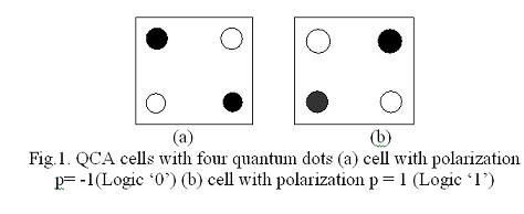
take up the diagonal positions. Binary levels are represented
by the positions of the electrons inside the cell unlike
the voltage or current levels as in the CMOS. Figure 1 show
the structures of quantum cell with two different polarizations
(electrons are shown with black filled circular dots).
Majority gate and Inverter are the two basic logic devices
of QCA. Fig.2 shows the structure of the majority gate with
3 inputs, driver cell and output cell. Computation starts
by driving the driver cell to the lowest energy state. Input
cell changes its state by the signal which arrives towards
the driver cell. Driver cell always gets the binary value
of majority of input signals since it is where the repulsion
for the mobile electrons in driver cell is at minimum and
output follows the state of driver cell.
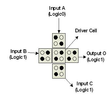
Fig.2 Majority Gate
The logic function for the majority gate is given by M(a,b,c)
= ab+bc+ca with a, b, c as boolean variables. In this way
two input AND, OR gates can be designed by keeping the third
variable as either 0 or 1 respectively.
Inverter is the other basic logic device of QCA. If cells
are placed diagonally to each other then they will have
opposite polarizations. QCA Inverter is designed by this
characteristic, such as shown in Fig. 3.
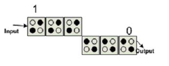
Fig.3. QCA Inverter
QCA Clocking:
In the case of QCA, the clock signal modulates the inter
dot barrier. QCA designs rely on a set of 4 clocks, phase
shifted with respect to each other. Clock is used to .push.
information from inputs to the output by modifying the cell
tunneling energy.QCA circuits have a four phase clock as
against the CMOS which has only two states high and low
and all the four phases have a phase shift of 90°, as shown
in Fig. 4. Power to the QCA circuit comes from the clock
itself unlike external power supply in case of CMOS. To
assign the clock, the QCA circuit is divided into four sub
arrays and a single potential modulates the inter-dot barriers
in all the cells present in given array. Clock feature allows
the sub array to perform a certain calculation at which
it does not have influence from its successor and it acts
as input to the next sub array, adding the feature of pipelining.
The four phases of clock correspond to switch, hold, release,
and relax. In Switch phase, the barriers are raised and
the QCA cells become polarized according to the state of
input drivers. In the Hold phase, the barriers are kept
high so that the cells in that sub array retain their values.
During the Release phase, the barriers are lowered and the
cells are allowed to relax to unpolarised state. In the
final relax phase the barriers kept on low and the cells
remains unpolarised.
Power Dissipation in QCA:
Unlike computation mechanisms that involve the transfer
of electrons, as in CMOS gates, QCA computation does not
involve electron transfer between adjacent QCA cells. Hence
power dissipation is very less in circuits designed with
QCA cells. Since only few electrons are involved in QCA
computations, it is susceptible to thermal issues. Therefore
it is important to consider power as an important parameter
during the QCA design process. The power loss in clocked
QCA circuits are classified as switching power and leakage
power. Leakage power loss is independent of input states
and occurs when the clock energy is raised or lowered to
polarize or depolarize a cell. Switching power dependents
on input data and occurs when the cell changes the state.
Total power loss can be controlled by varying the rate of
change of transitions in the clocking function.
|