Intel foundry to challenge TSMC and Samsung domination with range of innovations
Intel Foundry finally takes-off for a giga-range of wafer production in terms of scale and provides roadmaps to make up to 14A (1.4 nm) chips covering growing markets such as AI server market.
Intel also confirmed that they are on schedule with their ambitious plan to introduce five new manufacturing nodes within four years, known as the five-nodes-in-four-years (5N4Y) process roadmap. This plan includes the industry's first backside power solution. The company's leaders anticipate that Intel will regain its position as a leader in semiconductor manufacturing with the release of the Intel 18A node in 2025.
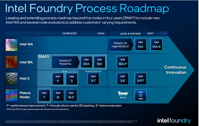
Pic: Intel foundry process roadmap (Source: Intel) The updated roadmap also outlines advancements in Intel 3, Intel 18A, and Intel 14A process technologies. One notable addition is Intel 3-T, which has been optimized for 3D advanced packaging designs using through-silicon vias (TSVs) and is nearing readiness for manufacturing. Additionally, the roadmap includes the introduction of new 12 nanometer nodes resulting from a recent collaboration with UMC, announced just last month. It has showcased some key groundbreaking advancements in semiconductor manufacturing such as backside plane power, glass subsrate and advances in 3D and 2.5 D packaging. More important is it is pitting itse...
Pic: Intel foundry process roadmap (Source: Intel) The updated roadmap also outlines advancements in Intel 3, Intel 18A, and Intel 14A process technologies. One notable addition is Intel 3-T, which has been optimized for 3D advanced packaging designs using through-silicon vias (TSVs) and is nearing readiness for manufacturing. Additionally, the roadmap includes the introduction of new 12 nanometer nodes resulting from a recent collaboration with UMC, announced just last month. It has showcased some key groundbreaking advancements in semiconductor manufacturing such as backside plane power, glass subsrate and advances in 3D and 2.5 D packaging. More important is it is pitting itse...
You've read this far — sign in to keep reading