Semiconductor tech by NVIDIA at GTC: GB200 super GPU chip and computational lithography breakthrough

Date: 19/03/2024
At its grand GTC event held on Mar 18th 2024 in San Jose,US, NVIDIA launched its latest lot more accelerated computing packed new AI GPU processor called NVIDIA GB200 Grace Blackwell Superchip. GB200 packs 208 billion transistors where the Blackwell-architecture GPUs are manufactured using a custom-built 4NP TSMC semiconductor process tech with two-reticle limit GPU dies connected by 10 TB/second chip-to-chip link into a single, unified GPU. NVIDIA GB200 Grace Blackwell Superchip connects two NVIDIA B200 Tensor Core GPUs to the NVIDIA Grace CPU over a 900GB/s ultra-low-power NVLink chip-to-chip interconnect. NVIDA claims the GB200 NVL72 provides up to a 30x performance increase compared to the same number of NVIDIA H100 Tensor Core GPUs for LLM inference workloads, and reduces cost and energy consumption by up to 25x.

GPU chip

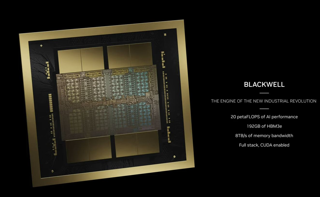
Pic: BLACKWELL GPU (source: NVIDIA)

Some of the key features include:
Higher AI inference: By integrating Micro-tensor scaling and NVIDIA’s advanced dynamic range management algorithms into NVIDIA TensorRT-LLM and NeMo Megatron frameworks, Blackwell to support double the compute and model sizes with new 4-bit floating point AI inference capabilities.

Data interconnect speed: The latest iteration of NVIDIA NVLink delivers a record 1.8TB/s bidirectional throughput per GPU, ensuring seamless high-speed communication among up to 576 GPUs for the most complex LLMs.

Higher reliability: Blackwell-powered GPUs feature a dedicated engine for reliability, availability and serviceability. Blackwell architecture also provide capabilities at the chip level to utilize AI-based preventative maintenance to run diagnostics and forecast reliability issues.

Security: Feature support for new native interface encryption protocols which are required for privacy-sensitive industries like healthcare and financial services.

Decompression Engine: An exclusive decompression engine supports the latest formats, accelerating database queries to deliver the highest performance in data analytics and data science.

GPU chip Pic: BLACKWELL GPU based system (source: NVIDIA)

NVIDIA GB200 NVL72 powered by GB200 is a a multi-node, liquid-cooled, rack-scale system that harnesses Blackwell to offer supercharged compute for trillion-parameter models, with 720 petaflops of AI training performance and 1.4 exaflops of AI inference performance in a single rack.

computational lithography platform for semiconductor fabs

For the semiconductor manufacturing world, TSMC and Synopsys are going into production with NVIDIA’s computational lithography platform to accelerate manufacturing and push the limits of physics for the next generation of advanced semiconductor chips. TSMC and Synopsys both have integrated NVIDIA cuLitho with their software, manufacturing processes and systems to speed chip fabrication, and in the future support the latest-generation NVIDIA Blackwell architecture GPUs.

computational Litho

Image source: NIVIDIA
To improve the semiconductor manufacturing process over current CPU-based methods, NVIDIA also introduced new generative AI algorithms that enhance cuLitho, a library for GPU-accelerated computational lithography.

NVIDIA said "Computational lithography is the most compute-intensive workload in the semiconductor manufacturing process, consuming tens of billions of hours per year on CPUs. A typical mask set for a chip — a key step in its production — could take 30 million or more hours of CPU compute time, necessitating large data centers within semiconductor foundries. With accelerated computing, 350 NVIDIA H100 systems can now replace 40,000 CPU systems, accelerating production time, while reducing costs, space and power." and also highlights "cuLitho has enabled TSMC to open new opportunities for innovative patterning technologies. In testing cuLitho on shared workflows, the companies jointly realized a 45x speedup of curvilinear flows and a nearly 60x improvement on more traditional Manhattan-style flows. These two types of flows differ — with curvilinear the mask shapes are represented by curves, while Manhattan mask shapes are constrained to be either horizontal or vertical."

NVIDIA also announced a new networking switch called the X800 series with capacity of end-to-end 800Gb/s throughput, NVIDIA Quantum-X800 InfiniBand and NVIDIA Spectrum-X800 Ethernet push the boundaries of networking performance for computing and AI workloads.

Jensen Huang, NVIDIA founder and CEO made these below comments while delivering his keynote:
Accelerated computing has reached the tipping point, general purpose computing has run out of steam.
The future is generative … which is why this is a brand new industry. The way we compute is fundamentally different. We created a processor for the generative AI era.
We’re going to train it with multimodality data, not just text on the internet, we’re going to train it on texts and images, graphs and charts, and just as we learned watching TV, there’s going to be a whole bunch of watching video.

nvidia