SK hynix and Gauss Labs presents 2 papers on AI semiconductor metrology at SPIE AL 2024
SK hynix and Gauss Labs have recently participated in the SPIE AL1 2024 conference, a prestigious international event focusing on advanced lithography and patterning technologies. At the conference, they presented two papers highlighting cutting-edge advancements in AI-based metrology, a critical aspect of semiconductor manufacturing.
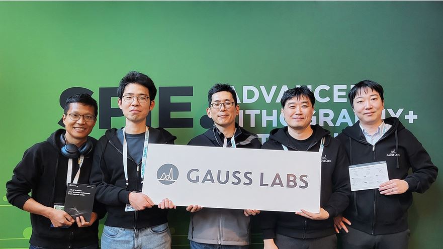
Figure: Gauss Labs CEO Mike Kim(center) poses with his colleagues Enhanced Prediction Accuracy: Gauss Labs introduced the "aggregated AOM3" algorithm, enhancing the prediction accuracy of its AI-based virtual metrology solution, Panoptes VM. This algorithm aggregates data from processing machines and chambers with similar patterns, addressing data scarcity issues and boosting prediction accuracy. Improved Process Variability: SK hynix utilized Panoptes VM for virtual measurements on over 50 million wafers, achieving a significant 29% improvement in process variability. This technology enables rapid virtual measurements, contributing to enhanced semiconductor yield and productivity. Universal Denoiser for Image Enhancement: Gauss Labs presented a "universal denoiser" algorithm designed to remove random variations (noise) from Critical Dimension Scanning Electron Microscope (CD-SEM) images. By employing AI, this denoiser improves measure...
Figure: Gauss Labs CEO Mike Kim(center) poses with his colleagues Enhanced Prediction Accuracy: Gauss Labs introduced the "aggregated AOM3" algorithm, enhancing the prediction accuracy of its AI-based virtual metrology solution, Panoptes VM. This algorithm aggregates data from processing machines and chambers with similar patterns, addressing data scarcity issues and boosting prediction accuracy. Improved Process Variability: SK hynix utilized Panoptes VM for virtual measurements on over 50 million wafers, achieving a significant 29% improvement in process variability. This technology enables rapid virtual measurements, contributing to enhanced semiconductor yield and productivity. Universal Denoiser for Image Enhancement: Gauss Labs presented a "universal denoiser" algorithm designed to remove random variations (noise) from Critical Dimension Scanning Electron Microscope (CD-SEM) images. By employing AI, this denoiser improves measure...
You've read this far — sign in to keep reading