Toppan and IBM to jointly research on EUV Photomasks for 2 nm semiconductor fabs
With the two leading semiconductor fab companies Intel, and Samsung moving to High NA EUV photolithography to fabricate 2 nm semiconductor chips, the other supported tools need to be also developed to withstand and support EUV light, mainly photomasks.
The photomasks, the stencil-like structures for light used in printing on semiconductor wafers do need to withstand the powerfull light in EUV range and also take care of diffraction and other optical issues.
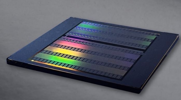
The leading photomask maker Toppan Photomasks has announced that it has entered into a joint research and development agreement with IBM related to the 2 nanometer (nm) logic semiconductor node, using extreme ultraviolet (EUV) lithography. This agreement also includes High-NA EUV photomask development capability on next-generation semiconductors. Based on this agreement, for a period of five years starting 1Q 2024, IBM and Toppan Photomask plan to develop photomask capability at the Albany NanoTech Complex (Albany, NY, USA) and Toppan Photomask's Asaka Plant (Niiza, Japan). Both IBM and TOPPAN Photomasks have a history of working together in developing advanced photomasks for nodes such as 45nm, 32nm, 22/20nm, and 14nm nodes during the period of 2005 to 2015, making both the companies to have expertise in this domain and appl...
The leading photomask maker Toppan Photomasks has announced that it has entered into a joint research and development agreement with IBM related to the 2 nanometer (nm) logic semiconductor node, using extreme ultraviolet (EUV) lithography. This agreement also includes High-NA EUV photomask development capability on next-generation semiconductors. Based on this agreement, for a period of five years starting 1Q 2024, IBM and Toppan Photomask plan to develop photomask capability at the Albany NanoTech Complex (Albany, NY, USA) and Toppan Photomask's Asaka Plant (Niiza, Japan). Both IBM and TOPPAN Photomasks have a history of working together in developing advanced photomasks for nodes such as 45nm, 32nm, 22/20nm, and 14nm nodes during the period of 2005 to 2015, making both the companies to have expertise in this domain and appl...
You've read this far — sign in to keep reading