The Godzillas of silicon chips: Extremely powerful advanced chips in the market

Date: 18/05/2024
Semiconductor experts predict an average one trillion transistors in a chip by 2030. That's clearly the growth curve following the famous Moore's Law. Let's look at some of the chips now in the market with highly dense number of transistors.

1 and 2: WSE 3 and WSE 2
The new Wafer Scale Engine(WSE) 3 and Wafer Scale Engine 2 are the world's largest integrated circuit chip for complex artificial intelligence (AI) computation applications training with very large AI databases as a single data core.

Cerebras Systems break its own record of designing a chip with larger transistor count compared to its previous Cerebras WSE-2. The new Wafer Scale Engine 3 (WSE-3), delivers double the performance without compromising on power consumption or cost. Engineered specifically for training the most extensive AI models, the WSE-3, built on a 5nm process, boasts 4 trillion transistors and 900,000 AI cores, enabling the Cerebras CS-3 AI supercomputer to achieve an impressive 125 petaflops of peak AI performance.

large chip

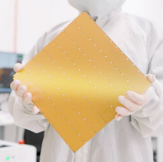
PIC: WSE 3

Key Features of WSE 3:

4 trillion transistors
900,000 AI cores
125 petaflops of peak AI performance
44GB on-chip SRAM
5nm TSMC process
External memory: 1.5TB, 12TB, or 1.2PB
Trains AI models up to 24 trillion parameters
Cluster size of up to 2048 CS-3 systems

Let's compare this with WSE 2: WSE-2 packs 2.6 trillion transistors and 40 gigabytes of on-chip memory with an active area of 46,225 mm2 fabricated on 300mm silicon wafers using TSMC's 7nm complementary metal-oxide semiconductor (CMOS) technology.

With a vast memory capacity of up to 1.2 petabytes, the CS-3 empowers the training of next-generation AI models, surpassing previous benchmarks such as GPT-4 and Gemini by tenfold. Its capability to handle models with up to 24 trillion parameters in a single logical memory space streamlines training workflows and enhances developer productivity. The CS-3 accommodates training from compact four-system configurations to full-scale operations with 2048 systems, enabling unprecedented advancements in generative AI.

The latest Cerebras Software Framework integrates seamlessly with PyTorch 2.0, facilitating the adoption of advanced AI models and techniques. Unique hardware acceleration for dynamic and unstructured sparsity accelerates training by up to 8x, underscoring Cerebras' commitment to innovation. Notably, the CS-3's superior power efficiency and streamlined software architecture require significantly less code compared to GPUs, reducing complexity and enhancing user experience.

Cerebras has garnered substantial interest across enterprise, government, and international cloud sectors, with a significant backlog of CS-3 orders. The strategic partnership between Cerebras and G42 has yielded remarkable results, culminating in the construction of Condor Galaxy 3, set to be one of the largest AI supercomputers globally. With its unparalleled capabilities and collaborative ventures, Cerebras is poised to revolutionize the AI landscape and drive the industry forward.

By embracing cutting-edge technology and fostering strategic partnerships, Cerebras continues to push the boundaries of AI innovation, paving the way for transformative advancements in machine learning and computational intelligence.

WSE 3 and WSE 2 are the world's largest integrated circuit chips for complex artificial intelligence (AI) computation applications training with very large AI databases as a single data core.

Cerebras Systems making these big chips by having multiple semiconductor wafers integrated using advanced semiconductor packaging and system design.

large chip

Pic above: WSE-2
These both chips are really giants compared to the rest below.

3. NVIDIA GB200

At its grand GTC event held on Mar 18th 2024 in San Jose,US, NVIDIA launched its latest lot more accelerated computing packed new AI GPU processor called NVIDIA GB200 Grace Blackwell Superchip. GB200 packs 208 billion transistors where the Blackwell-architecture GPUs are manufactured using a custom-built 4NP TSMC semiconductor process tech with two-reticle limit GPU dies connected by 10 TB/second chip-to-chip link into a single, unified GPU. NVIDIA GB200 Grace Blackwell Superchip connects two NVIDIA B200 Tensor Core GPUs to the NVIDIA Grace CPU over a 900GB/s ultra-low-power NVLink chip-to-chip interconnect. NVIDA claims the GB200 NVL72 provides up to a 30x performance increase compared to the same number of NVIDIA H100 Tensor Core GPUs for LLM inference workloads, and reduces cost and energy consumption by up to 25x.

GPU chip

Pic: BLACKWELL GPU (source: NVIDIA)

4. Apple M2 Ultra

The M2 Ultra from Apple packs 134 billion transistors with around 60 processor cores and is made using TSMC 5 nm technology node.

big

Image Source: Apple
M2 Ultra is the latest high peformance chip by Apple powering the new Mac Studio and Mac Pro desktops.
M2 Ultra features unified memory architecture to handle breakthrough 192GB of memory capacity and support 800GB/s of memory bandwidth. M2 Ultra has powerful CPU and large GPU. 32-core Neural Engine inside M2 Ultra handles 31.6 trillion operations per second.
M2 Ultra packs two M2 Max dies connected using Apple's UltraFusion packaging technology, which uses a silicon interposer to connect silicon dies with more than 10,000 signals, providing over 2.5TB/s of low-latency interprocessor bandwidth.
The media engine inside M2 Ultra has dedicated, hardware-enabled H.264, HEVC, and ProRes encode and decode, allowing M2 Ultra to play back up to 22 streams of 8K ProRes 422 video.
M2 Ultra integrate a display engine driving up to six Pro Display XDRs of 100 million pixels.
It also featues Secure Enclave and a hardware-verified secure boot and runtime anti-exploitation technologies to make the device secure.

5. AMD Instinct MI300X
Another chip beast in the market is AMD Instinct MI300X accelerator, the advanced accelerator for generative AI.

It has 13 chiplets stacked in 3D, 24 Zen CPU cores, graphic engine, and 8 stacks of HBM3 with total transistor count of 146 billion. It is the largest AMD chip in production. MI300 is 8x improvement in AI performance and 5x in performance per watt compared to its earlier Instinct MI250.

big

Image Source: AMD

6. Intel Data Center GPU Max 1550

Intel Data Center GPU Max 1550 which was formerly called as Ponte Vecchio packing 100 billion transistors is Intel’s highest density processor. It has 47 chiplets/tiles with up to 128 gigabytes (GB) of high bandwidth memory. Ponte Vecchiio which is called Intel GPU Max Series features 408MB of L2 cache and 64MB of L1 cache to increase throughput and performance. The Intel Data Center Max Series GPU, code-named Rialto Bridge successor to the Max Series GPU and is intended to arrive in 2024.

big

Image Source: Intel

7. NVIDIA H100 and A100
NVIDIA H100 and A100: Nvidia A100 has 54 billion transistors with silicon die size of 826 mm square and can execute 5 petaflops of performance. It has tensor cores and has up to 128 streaming multiprocessor (SMs) and 8192 FP32 CUDA cores.

NVIDIA H100 packs 80 Billion Transistors and has up to 144 streaming multiprocessors. Each SM is composed of up to 128 FP32 units which should give us a total of 18,432 CUDA cores. Other specs include:
big

Image Source: nVidia
big

Image Source:nVidia
These chips feature 4 Fourth-generation Tensor Cores per SM, 528 per GPU 80 GB HBM3, 5 HBM3 stacks, 10 512-bit Memory Controllers and 50 MB L2 Cache.

8. Intel Core 14th Gen i9-14900KS

Though hesitantly listed this processor in this article. It's the most latest desktop processor by Intel with 24 cores and 32 threads. It can work upto a frquency up to 6.2 GHz. The exact transistor count is not provided, it can be estimated in the range of 30 Billion+.

big

Image Source: Intel


9. Snapdragon X Elite
The most latest Snapdragon X Elite by Qualcomm is a new 4.3 GHz, 12-core, 64-bit Arm processor is 2X better in performance compared to Intel's Core i9-13980HX of x86 Architecture and some of the Apple's PC and notebook processors such as Apple M2. The exact transistor count is not provided, it can be estimated in the range of 25-30 Billion.

big

Image Source: Qualcomm

PS: This article was updated on 18th May 2024 with ranking updated to original article posted on 30/10/2023. MPU

Author: Srinivasa Reddy N
Header ad