1nm semiconductor chips: Research references points 1nm GAA FETs is achievable

Date: 26/06/2023
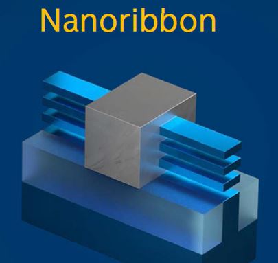
When the channel width of the FinFET goes below 3 nm, the present metal gate structure fail to reliably control the flow of electrons in the channel. To achieve efficient switching you need the metal gate all around, that leads to gate all around FETs (GAA FETs). Then the channel takes the shape of wire or a sheet. Another challenge in 1nm is availability of less number free electrons and holes in pure silicon-channel, irrespective of it is strained or not. In an extraordinary human effort to control electron movement in semiconductor structure with few tens of atoms in hundred percent reliable manner, both switching on and switching off is extremely challenging. Researchers in their quest to increase the density of transistors, they are finding Silicon alternates such as Germanium and other compound semiconductor materials offering higher free -charge density. Silicon Germanium (Si-Ge) nano sheets are very effectively used as channel material in many of latest commercially successful and under-development research. The challenge here is to manufacture such devices in mass volumes with no or least variance from chip to chip.

nano wire


To achieve atomic level building of 1 nm transistor switching elements, the semiconductor engineering researchers are using epitaxial deposition and atomic layer deposition techniques. Here in this article, I try to collate the progress of research efforts by individual semiconductor engineering researchers, exclusive semiconductor research organizations and companies in this area.

Reference1:
In an article/paper titled "Ge/Si multilayer epitaxy and removal of dislocations from Ge-nanosheet-channel MOSFETs", authors talks about structural mechanisms used to achieve required gate control and electrical properties of the switch.

These researchers have used techniques such as:
Large lattice mismatch Ge/Si multilayers were intentionally grown as the starting material rather than Ge/GeSi multilayers to acquire the benefits of the considerable difference in material properties of Ge and Si for realizing selective etching. Flat Ge/Si multilayers were grown at a low temperature to preclude island growth. The shape of Ge nanosheets was almost retained after etching owing to the excellent selectivity.

Authors also said "Germanium and III–V compounds are known to effectively improve the electron mobility of transistor channels. They grew Ge(40 nm)/Si(25 nm) layers epitaxially on 40-nm-thick Si substrates and a buried oxide (BOX) thickness of 150 nm by LPCVD using GeH4 and SiH4 gases.

For details click the paper titled Ge/Si multilayer epitaxy and removal of dislocations from Ge-nanosheet-channel MOSFETs

Reference2:

In another article/paper titled "Mapping of the mechanical response in Si/SiGe nanosheet device geometries", Authors Conal E. Murray, Hanfei Yan, Christian Lavoie, Jean Jordan-Sweet, Ajith Pattammattel, Kathleen Reuter, Mohammad Hasanuzzaman, Nicholas Lanzillo, Robert Robison & Nicolas Loubet have reported synchrotron x-ray diffraction-based non-destructive nanoscale mapping of Si/SiGe nanosheets for gate-all-around structures. They have identified two competing mechanisms at different length scales contributing to the deformation. One is consistent with the in-plane elastic relaxation due to the Ge lattice mismatch with the surrounding Si. The second is associated with the out-of-plane layering of the Si and SiGe regions at a length scale of film thickness.

Researchers said "Nanosheet samples were fabricated by IBM Research at the 300 mm Nanotech facility in Albany NY. Epitaxial growth of the SiGe layers was performed on 300 mm diameter, (001)-oriented silicon wafers in a commercially available, rapid-thermal chemical vapor deposition reactor."

For details click the paper titled Mapping of the mechanical response in Si/SiGe nanosheet device geometries

Reference3:

In the paper titled "SiGe and Si Gate-All-Around FET Fabricated by Selective Etching the Same Epitaxial Layers", authors Wei-Yuan Chang; Guang-Li Luo; Yi-Shuo Huang; Chun-Lin Chu; Yao-Jen Lee; Bo-Yuan Chen; Chun-Hsiung Lin; Wen-Fa Wu; Wen-Kuan Yeh said in the abstract that "SiGe Gate-All-Around (GAA) p-FETs and Si GAA n-FETs were fabricated on the same Si/SiGe multilayer epitaxial wafer for the first time. The SiGe and Si multi-bridge channels (MBC) were respectively formed by Si interlayers selective etching and SiGe interlayers selective etching. For improving interface quality between Si and high-k, both Si and SiGe surfaces were processed with H2O2 treatment and forming gas (FG) annealing before the high-k gate deposition. The process scheme in this work can be easily applied to integrate SiGe GAA p-FETs and Si GAA n-FETs on the same wafer."
For details click the paper titled SiGe and Si Gate-All-Around FET Fabricated by Selective Etching the Same Epitaxial Layers

ALD and Epitaxial growth
ALD

ALD (atomic layer deposition) and epitaxial growth of nanostructures is enabler of making chips using new hetergenous channel materials. If you're looking to learn more on the atomic layer deposition, here is a little old but very nice article written by Robert N. Castellano President, The Information Network. The beauty of ALD is it works at lower temperatures compared to other processes. For details click the Article titled ATOMIC LAYER DEPOSITION TRENDS AND MARKETS

ASM International and Applied materials makes semiconductor equipments for epitaxial deposition and ALD.You can find some technology readings in the below pages of ASM International.
Epitaxy Page explains " Epitaxy, often called Epi, is the process of depositing highly controlled silicon-based crystalline films, a critical process technology for creating advanced transistors and memories, and for wafer manufacturing" at: https://www.asm.com/epitaxy
ALD page explains "ALD is a surface-controlled layer-by-layer process that results in the deposition of thin films one atomic layer at a time. Layers are formed during reaction cycles by alternately pulsing precursors and reactants and purging with inert gas in between each pulse." at: https://www.asm.com/ald

epitaxy


On the various process steps used in fabricating nanosheet MOSFETs, the leading semiconductor equipment maker Lam Research explains "The GAA transistors are fabricated by first growing a superlattice of alternating Si and SiGe epitaxial layers, which form the basis for the nanosheets. Critical steps include deposition of an inner dielectric spacer to protect the source/drain regions and define the gate width, as well as the channel release etch to remove the sacrificial layers. That space left by removal of the sacrificial layers then needs to be filled with the gate dielectric." The page can accessed at: https://newsroom.lamresearch.com/FinFETs-Give-Way-to-Gate-All-Around
Last and very relevant information to know is, there is one Indian born researcher named Dr. Jagdish Narayan who has done extra-ordinary work in epitaxial deposition of materials who has contributed significantly to material process and material research not only semiconductor domain but also in many of aspects of engineering. Complete reading of his work help to gain deep knowledge in the area of deep node chip making below 5nm including silicon photonics.

epitaxial


Narayan is the John Fan Family Distinguished Chair Professor in the Department of Materials Science and Engineering with courtesy faculty appointments in Physics and EFC at NC State. He is Distinguished Visiting Scientist at Oak Ridge National Laboratory. He graduated from India’s IIT, Kanpur in 1969, Narayan continued his studies at the University of California, Berkeley, and obtained his MS (1970) and PhD (1971) degrees in a record time of two years.
His invention of domain matching epitaxy across the misfit scale has revolutionized epitaxial integration of nano-structured materials in the form of nanolayers, nanodots, and nanorods on practical substrates such as silicon. The DME paradigm has led to the integration of exciting new materials, which include perovskites such as NdNiO3, vanadium oxide, titanium oxide, nickel oxide, and most recent novel topological insulator (Sr3SnO) and bismuth ferrite with unique magnetic properties
Read his research profile at:
https://www.mse.ncsu.edu/narayan/research/

https://www.mse.ncsu.edu/people/narayan/

Author: Srinivasa Reddy N
Header ad