AI EDA on Cloud, a super-fast emerging market opportunity in semiconductor chip design

Date: 26/06/2023
Semiconductors and electronics are the central driving force in today's AI systems. And this industry is the front-runner in using AI to design better chips and better electronics. Whether you call it AI or high-performance computing or hyperscale systems, computer started performing better than human experts in chip design. Semiconductor chip design is becoming more and more software centric. VLSI chip designers hardly go deep into semiconductor fabrication technologies such as gate all around (GAA) FET, interconnect and many such deep node techs, as long as EDA companies take care of those changes in their latest tools.

AI CLOUD EDA


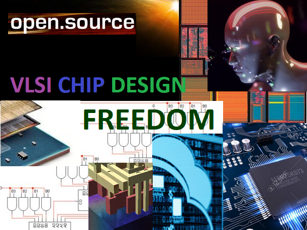
Something to cheer about this trend is; open source is fast evolving in this area along with extraordinary performance enhancements by proprietary paid third-party software from leaders in this domain . A kind of inevitable EDA tools from Synopsys, Cadence, Ansys, Keysight and Siemens have a new competitor in the form of open source EDA tools mainly driven by Google and other cloud-based systems. Open Source is becoming more and more inevitable as much as top-3 paid products if not so much in software tools but in IP. A quick example is RISC-V vs ARM’s latest processor IP and very proprietary Synopsys’ ARC. This supports the thought of "More democratic research environment is better than having this powerful technology controlled by a small number of corporations" stated in a recent article titled Big Tech Isn’t Prepared for A.I.’s Next Chapter; Open source is changing everything

When SOC chip design move from 7 nm to 3 nm, the design data grows by nearly 4 times and even more in some cases. You need extraordinary high-performance computing environment to run that data. Since each chip design company spends 100s of millions of dollars in designing complex SOC chip, it is natural to evaluate third-party AI tools along with use of open-source tools. It is too expensive and resource-prone to own high performance computing servers for SOC chip design companies. So using EDA on cloud is irresistible option. Some of the experts in the industry calling AI EDA on cloud a necessity. Since today's cloud computers are Hyperscale, you get all the latest AI resources available updated with the time. They can also work in hybrid mode where they can run highly compute intensive AI loads on cloud, and some mature and protected VLSI software on their internal systems.

Let's look at what are the popular cloud based AI sources available for VLSI semiconductor chip design industry.

Google:
Google cloud is most sought-after computing-environment by open-source chip-design community. The fact is Google itself is into semiconductor chip design and has designed chips using a new AI-based processes saving time, and also improving typical PPA performance of chips. Google designs its chips Tensor SoC completely on the cloud. They have extensively used neural networks in VLSI chip design processes such as placement and routing. Trained AI models can place and route IP blocks more efficiently than chip design experts. Read the article titled: Chip Design with Deep Reinforcement Learning

Google has made available some of the tools and learning openly available for designing complex SOC chips. Sashi Obilisetty Chief Architect, Silicon Solutions and Mark Mims have written an article titled Never miss a tape-out: Faster chip design with Google Cloud where they have clearly explained how to leverage some innovative processes to speed up complete chip design activity with successful tape out.

AI EDA cloud
Image Source: cloud.google.com

Google also put up an article titled All Google chip design now takes place in the cloud and a YouTube video how it moved all the EDA tools from an exclusive computer to cloud.

Another worthy article for learning is Scale your EDA flows: How Google Cloud enables faster verification from Sashi Obilisetty and Mark Mims.

Google in partnership with GlobalFoundries, skyWater technology and Efabless provides a single environment to design and tape out your own chip, where the group provides process design kits and toolchains, where you not only design and also fabricate the chip. Visit the page title Build your own silicon

Amazon AWS:
Complete open source chip design is possible due to various organizations offering tools and software to work on Amazon cloud. Service such as NICE DCV desktop Cloud visualization, Amazon EC2, S3, secrets manager, certificate manager various such services can be used to run chip design workloads on cloud. Amazon AWS exclusively support open source EDA tools and from leading EDA companies. The number one EDA vendor Synopsys helps VLSI design engineers to deploy their EDA workload on Amazon Web services securely.
Synopsys said it offers Black Duck and Coverity integrations with support for AWS CI tools (CodeBuild, CodePipeline, CodeStar) and Elastic Kubernetes Service (EKS).

There's a blog on AWS titled "Open-Source Chip Design on AWS" talk about how open source EDA chip design can leverage Amazon AWS . Access the page at https://aws.amazon.com/blogs/industries/open-source-chip-design-on-aws/
Processor IP vendor ARM has extensively used Amazon AWS to run production-grade EDA software on cloud . ARM has migrated its EDA workloads to AWS and used services such as AWS Graviton2-based instances. ARM has effectively used AWS services to do chip verification to run simulations in parallel. Chip designers can leverage scalable compute power available on cloud by running stimulations in parallel, reduce iteration time. ARM has used AWS compute optimiser, and machine learning based services to recommend optimal Amazon EC2 instance types.
AI EDA cloud
Image Source: aws.amazon.com


Microsoft Azure:
Microsoft Azure is another cloud services vendor to handle EDA workloads for companies such as AMD where they have used Siemens Calibre platform to run on Microsoft Azure. Synopys is also fully leveraging Microsoft Azure in offering its cloud EDA services. Azure runs exclusive EDA optimized cloud environment. Microsoft Azure talks about having rich partner ecosystem involving chip design houses, foundries, packaging and testing companies and also system integrators. AI-based EDA software start-ups can use these cloud environments to initially test and launched the product.
Don’t ignore the leader IBM in this area. Cadence is offering its public cloud based EDA since 2016. It is using R&D workloads in IBM Cloud. Cadence had used IBM Spectrum LSF as the HPC workload scheduler and to perform more regressions.
The advantages of AI-based cloud products in EDA domain includes such as scalable computing environment, global availability of services, high-performance, and also controlled cost.
When it comes to trust and security, cloud-based services were always questioned, but due to the benefits they offer security and trust takes little backseat. The benefit of today's cloud-based EDA is it's AI-embedded. Small startups in VLSI can gain design advantage by using cloud-based EDA having most latest features such as machine learning algorithms and lot more.
Google Cloud, Amazon AWS and Microsoft Azure, and IBM have exclusive and focused services on EDA industry. If you looking for cloud services for a complete chip design or to run some part of computing load of design; a range AI based EDA cloud offerings allows you to opt flexible and customized deployment model as per your needs. Since cloud computing service providers and EDA companies collaborate closely, mutual customers can transfer EDA workloads to cloud by taking assistance from these companies to reap the benefits and get time and resource advantage.
To design next wave of semiconductor chips for devices such as Apple Vision Pro and most advanced AI chips, AI EDA on cloud offers significant advantage over previous processes. Just simply to put, it is "AI for AI". In my future series of articles I will delve deep into other various resources available on cloud not only for chip design but for the complete electronics design.

Some more references for you:

Azure for the semiconductor industry

AWS and Arm Demonstrate Production-Scale Electronic Design Automation in the Cloud

Cloud-based chip design for national security achieves key milestone

Accelerate silicon design innovation on Azure with Synopsys Cloud

Cloud-based chip design for national (U.S.) security achieves key milestone

Synopsys is offering cloud based EDA tool for a full commercial tape out of chips.

Author: Srinivasa Reddy N
Header ad