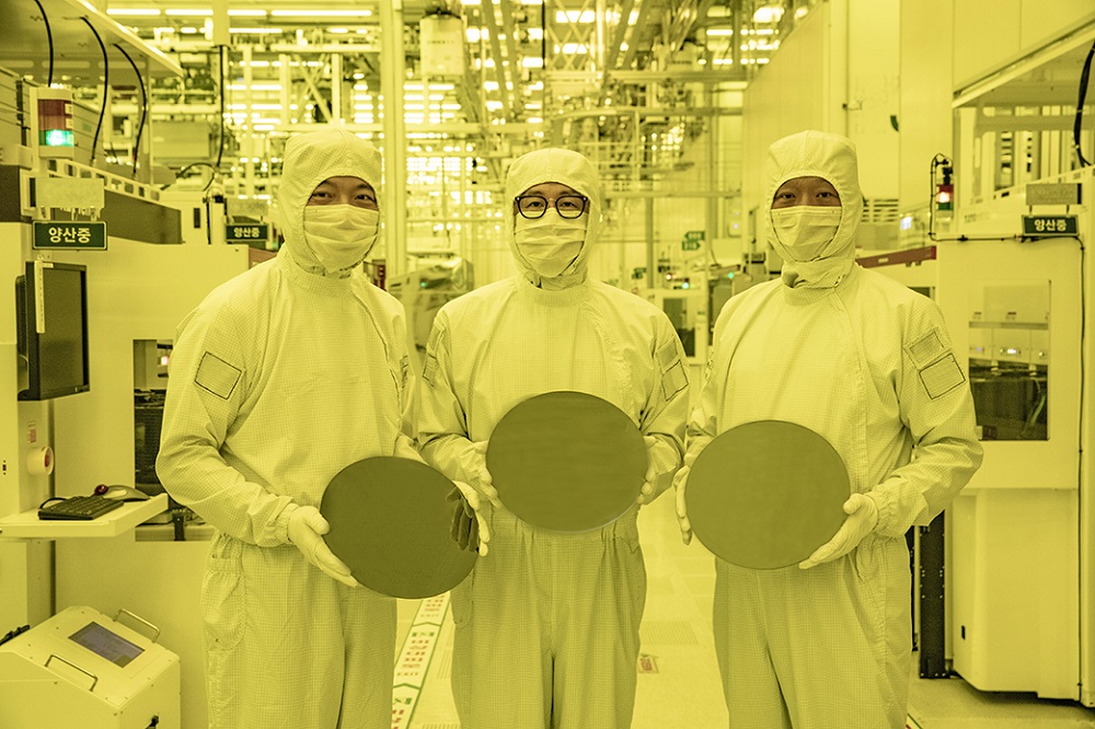
Samsung IP eco supported by EDA Cos Cadence and Synopsys

Date: 16/06/2023
While the node shrinks from 5 nm to 3 nm, VLSI design data growth gets compounded and complexity grows in Giga range in terms of data, testing, verification, and number of functions and variables.
So it's not just partnering with semiconductor/electronics design automation firms, nearly co-working, co-executing with interdisciplinary experts working in sync across semiconductor engineering, software design tools, Silicon IP experts, and mutually accepted standards stakeholders.

To keep IP risk-free and to ensure successful first tape-out of chips EDA firms Synopsys and Cadence are closely collaborating with Samsung foundry to ensure best support for common customers. In a separate releases both Synopsys and Cadence have announced delivering silicon VLSI IP for advanced nodes of Samsung's semiconductor foundry.

3nm chips


Synopsys to enhance its IP offering for Samsung's advanced 8LPU, SF5, SF4 and SF3 processes and includes Foundation IP, USB, PCI Express, 112G Ethernet, UCIe, LPDDR, DDR, MIPI and more.

Synopsys said it will also optimize IP for Samsung's SF5A and SF4A automotive process nodes to meet stringent Grade 1 or Grade 2 temperature and AEC-Q100 reliability requirements, enabling automotive chip designers to reduce their design effort and accelerate AEC-Q100 qualification. The auto-grade IP for ADAS SoCs will include design failure mode and effect analysis (DFMEA) reports that can save months of development effort for automotive SoC applications.

"Our extensive co-optimization efforts with Samsung across both EDA and IP help automotive, mobile, HPC, and multi-die system architects cope with the inherent challenges of designing chips for advanced process technologies," said John Koeter, senior vice president of product management and strategy for IP at Synopsys. "This extension of our decades-long collaboration provides designers with a low-risk path to achieving their design requirements and quickly launching differentiated products to the market."

"Samsung's longstanding collaboration with Synopsys, as our primary IP partner, has benefited our mutual customers by providing access to high-quality IP through each generation of Samsung's technology advancements," said Jongshin Shin, corporate executive vice president of Foundry IP Development at Samsung Electronics. "Extending this partnership across Samsung's full range of advanced nodes gives designers access to the industry's broadest IP portfolio, enabling them to meet the performance, power and area requirements of their target applications with less risk and faster time-to-market."

Synopsys IP available or in development for Samsung processes includes logic libraries, embedded memories, TCAMs, GPIOs, eUSB2, USB 2.0/3.0/3.1/4.0, USB-C/DisplayPort, PCI Express 3.0/4.0/5.0/6.0, 112G Ethernet, Multi-Protocol 16G/32G PHYs, UCIe, HDMI 2.1, LPDDR5X/5/4X/4, DDR5/4/3, SD3.0/eMMC 5.1, MIPI C/D PHY, and MIPI M-PHY G4/G5.

Cadence Design Systems has also announced the signing of multi-year agreement with Samsung Foundry to expand the availability of Cadence’s design IP portfolio on Samsung Foundry’s SF5A process technology, the latest 5nm process variant to support automotive applications.
Cadence said its joint customers can obtain a complete design IP solution from Cadence, a collaborative partner in the Samsung Advanced Foundry Ecosystem (SAFE), including 112/56/25/10G PHY/MAC, PCI Express (PCIe) 6.0/5.0/4.0/3.1 PHY/Controller, Universal Chiplet Interconnect Express (UCIe) PHY/Controller, USB3.x PHY/Controller and a complete PHY and controller offering for GDDR6 and DDR5/4.

Cadence and Samsung have also agreed to enable latest DDR5 8400+ and GDDR7 solutions on Samsung Foundry’s advanced SF3 technology to support its customers for a future-proof migration path who are designing chips for generative AI/ML, hyperscale, and high-performance computing (HPC) applications using high-performance, high-bandwidth memory interface.

Cadence said it provides full subsystem delivery with integrated PHY and controller IP to simplify integration, minimize risks, and enable faster time to market.

“Cadence and Samsung have been collaborating closely on Samsung EDA and IP ecosystem enablement for years. Through this new multi-year IP expansion plan, we further solidify our commitment to empowering joint customers with access to a complete design IP portfolio on SF5A technology as well as the leading DDR5 8400+ and GDDR7/6 solutions on SF3,” said Jongshin Shin, EVP of Samsung Foundry and Head of IP Ecosystem.

“Cadence is committed to expanding our IP portfolio to address our customers’ evolving design requirements,” said Rishi Chugh, vice president of product marketing in the IP Group at Cadence. “Through this collaboration with Samsung, we can deliver a rich set of high-performance IP with competitive PPA that meets the most demanding requirements for HPC, AI/ML, networking, storage, and automotive applications. Developing the latest GDDR7 IP on SF3 demonstrates our leadership in this market segment.”

Cadence also confirmed active customer engagements for these IP cores are currently underway.