Germanium Tin alloy as channel material for <2nm CMOS

Date: 07/06/2023
Multiple research agencies are working on new channel material to replace silicon in deep nodes so that Moore's Law can work upto 1nm. Germanium-Tin alloy is been tested and found to be one of the choice of material by team of researchers and scientists from CEA Leti, France; ForschungsZentrum Jülich, Germany; the University of Leeds, United Kingdom; IHP- Innovations for High Performance Microelectronics, Frankfurt (Oder), Germany, and RWTH Aachen University, Germany.

This team could fabricate new type of transistor from a germanium-tin alloy. They have demonstrated electrons and other charge carriers can move faster in Germanium-Tin than in Silicon or Germanium, enabling lower operation voltages and smaller footprints in vertical than in planar devices. These are compatible with exising CMOS process, making them an option for low-power, high-performance chips and possibly quantum computers.

Ge Sn


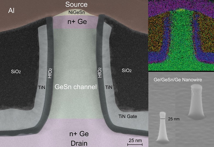
Mobility of electrons in Germanium–Tin transistors is 2.5 times higher than a comparable transistor made of pure Germanium. Germanium and Tin come from the same periodic table group as Silicon, these transistors could be integrated directly into conventional silicon chips with existing production lines, said CEA Leti in its release.

A recently published paper in Nature Communications Engineering, Vertical GeSn Nanowire MOSFETs for CMOS Beyond Silicon, notes that “GeSn alloys offer a tunable energy bandgap by varying the Sn content and adjustable band off-sets in epitaxial heterostructures with Ge and SiGe. In fact, a recent report has shown that the use of Ge0.92Sn0.08 as source on top of Ge nanowires (NWs) enhances the p-MOSFET performances.”

“In addition to their unprecedented electro-optical properties, a major advantage of GeSn binaries is also that they can be grown in the same epitaxy reactors as Si and SiGe alloys, enabling an all-group IV optoelectronic semiconductor platform that can be monolithically integrated on Si,” the paper reports.

CEA-Leti has delivered the epitaxial stacks. Epitaxy is carried out on a very ordered template, a silicon substrate, with a very precise crystal structure. By changing the material, CEA-Leti duplicated its diamond crystalline structure in the layers it put on top.

“Epitaxy is the art of making multi-layers by duplicating the original structure and is performed at low temperature with gaseous precursors in a chemical vapor deposition (CVD) reactor,” said Jean-Michel Hartmann, a CEA Fellow and team leader, group-IV epitaxy at CEA-Leti.

Depositing this kind of stack and mastering the epitaxial-layer growth is an extremely complex step in a process flow requiring patterned cylinders and conformal gate stack deposition – in short, manufacturing the entire device. CEA-Leti, one of the few RTOs globally that is able to deposit such complex in-situ doped Ge/GeSn stacks, performed that part of the joint research reported in the paper.

“The collaboration demonstrated the potential of low-bandgap GeSn for advanced transistors with interesting electrical properties, such as high carrier mobilities in the channel, low operating voltages and a smaller footprint,” explained Hartmann, a co-author of the paper. “Industrialization is still far away. We are advancing on the state of the art and showing the potential of germanium tin as a channel material.”

Ge Sn


Jean-Michel Hartmann received the Electronics and Photonics Division Award at the recent Electrochemical Society conference in Boston.

Hartmann is a CEA Fellow at CEA-Leti, leader of the working group in IV epitaxy, and the SSURF department’s scientific director. His research focuses on the reduced pressure chemical vapor deposition of group-IV semiconductors for nanoelectronics and optoelectronics.

Author: Srinivasa Reddy N
Header ad