Applied to invest 4 billion to set up collaborative semiconductor research center

Date: 23/05/2023
Semiconductor equipment tool vendor Applied Materials announced investment of US$ 4 billion for next seven years to build what it calls world's largest semiconductor manufacturing research facility, where the leading semiconductor chipmakers, semiconductor ecosystem partners as well as academic researchers from universities can collaborate with Applied Materials in developing processes and the equipment in making angstrom (1nm range) scale semiconductor chips. The collaborative idea is to reduce the design turnaround time for new technology innovations in chipmaking.

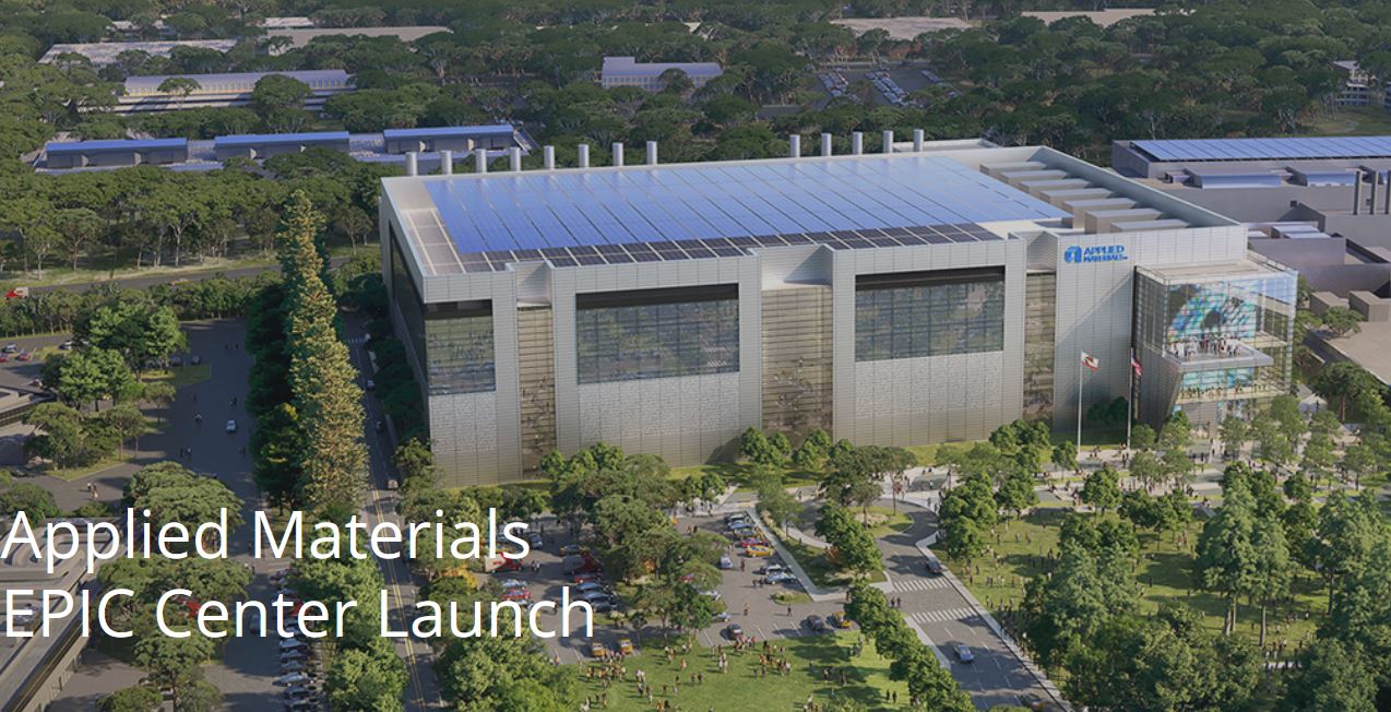
Applied plan to locate the new facility in the Silicon Valley, US with a physical space of 180,000 square ft state-of-the-art cleanroom. This new facility is called as EPIC Center. Applied plan to complete the new facility by 2026.

Applied Materials EPIC


Applied release states "Designed from the ground up to accelerate the pace of introducing new manufacturing innovations, the new EPIC Center is expected to reduce the time it takes the industry to bring a technology from concept to commercialization by several years, while simultaneously increasing the commercial success rate of new innovations and the return on R&D investments for the entire semiconductor ecosystem."

"While semiconductors are more critical to the global economy than ever before, the technology challenges our industry faces are becoming more complex,” said Gary Dickerson, President and CEO of Applied Materials. “This investment presents a golden opportunity to re-engineer the way the global industry collaborates to deliver the foundational semiconductor process and manufacturing technologies needed to sustain rapid improvements in energy-efficient, high-performance computing."

"The "angstrom era" of chipmaking requires new foundational manufacturing technologies that are orders of magnitude more complex than those used today. This increased complexity drives higher R&D and manufacturing costs, while lengthening the time it takes to develop and commercialize new semiconductor technology through high-volume manufacturing. Further hurdles include a critical shortage of technical talent needed by the industry and the pressing need to reduce the carbon intensity of the electronics industry." stated in the Applied' release.

Chipmakers can have their own dedicated space within Applied' equipment supplier facility, so that they don't need to wait for the equipment to get installed in their facility to test run the chip-taping.

Universities can use Applied’s new platform to the full range of industrial-scale capabilities to validate their academic research idea, increasing the success rate of innovations and reducing the time and cost of commercializing new technologies.

"We're all-in as an asset to industry and to the nation as we seek to regain global pre-eminence in semiconductor manufacturing, research and development,” said Arizona State University President Michael Crow. “Applied Materials is providing extraordinary leadership to accelerate innovation and commercialization of foundational manufacturing technologies that will define the future of how chips are made. And as we continue to innovate in that process, ASU will bring research expertise and help create the future innovation and manufacturing talent pipeline that will be critical over the long term."

A number of leading semiconductor and computing companies such as AMD, IBM, Intel, Micron, Nvidia, Samsung, TSMC and Western Digital, and academic researchers have commented on Applied's announcement.

Listen to comments from chipmakers and academic researchers in the page:
https://www.appliedmaterials.com/us/en/epic-center.html

Author: Srinivasa Reddy N
Header ad