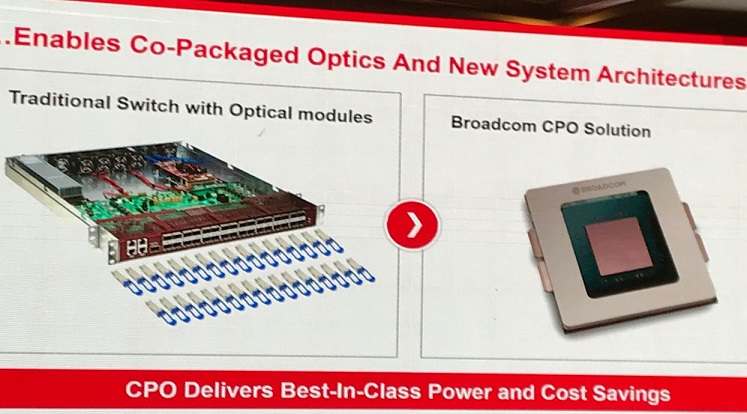
Chiplet-driven, More-than-Moore way creating exponential growth for semiconductor packaging

Date: 07/12/2022
While the monolithic semiconductor chips getting denser and denser with the Moore's law progressing towards 1 nm technology node, the cost of developing complete system on chip is alarmingly rising in the nodes of 3 nm and lower. It is estimated to cost around $ 750 million to design a monolithic SoC chip in the nodes of 2 nm. Although shrinking is achieved but some of the other benefits of Moore's Law are missing at <7nm nodes. So the better economic alternative is to go for heterogeneous integration of multiple monolithic semiconductor chips called chiplets in 3-dimensional semiconductor packaging and also using advanced interconnect technologies. In fact, chiplet-era already started by leading chip vendors Intel, Broadcom, Samsung and Micron, who have launched successful products in the market.

semicon package

Due to this major tech-driven shift from System-on-Chip to System-in-Pacakge, semiconductor packaging industry is estimated to grow faster than semiconductor chip fabrication. More and more semiconductor companies to offer their monolithic integrated circuit devices in the form of chiplets. The system designer of the end product to pick various chiplets for the targeted application, and outsource that design to semiconductor fabrication service provider to assemble and test the product. These service providers are called as OSAT - Outsourced Semiconductor Assembly and Test companies. The demand for OSAT companies is increasing exponentially. In this article, I try to cover various business opportunities, trends and latest technologies in semiconductor packaging after recently attending IEEE' Electronics Packaging Society (IEEE EPS-IESA) annual workshop held in Bangalore, India on Dec 1st and 2nd of 2022. Dr. Tummala Rao, a veteran in semiconductor packaging was there at the event sharing his thoughts on the industry and giving expert advise to faculty at IITs in taking up research work in this area. Dr. Tummala Rao is a distinguished and an endowed chair professor in electrical and computer engineering and in materials science and engineering at Georgia Institute of Technology, US.

The total global market for OSAT can be estimated around US$ 50-US$ 60 billion in the year 2023. The global market for 3 dimensional semiconductor packaging is estimated around $ 10-12 Billion in the year 2022, with annual growth rate estimated around more than 20%. In 2023, around 10 to 20% of advanced node designs directed towards Chiplet based multi-die packaging applications. There is an extraordinary demand for CAD/EDA design automation software tools to support the design of system in package. The need and want of market is so much, the EDA companies lagging in fulfilling them.

Geographically speaking, the present market is dominated by Taiwan and China (top 8 OSAT companies in the world headquartered in these two regions) Japan, South Korea, Singapore, Malaysia and Philippines also hold a significant share in this market. Amkor is lone company from US ranked in the top 10 OSAT list. Though, India hardly has 1% share in this market, there is a huge potential and growth ahead for India as per experts at the event. The support from the Government to this industry is no less than chip-fabrication.

Semiconductor packaging is more of the interdisciplinary science than a specific engineering with heavy focus on system approach. There is severe human resource shortage in semiconductor packaging around the world. I will write a separate article covering deeper into the subject of skill and talent shortage.

semicon package science

It won't be a shock, if lot more OSAT companies emerges with annual turnover of tens of billions dollars within next 10 years. Semiconductor foundries do not want to give away that big pie to packaging industry, so some of them are diversifying into OSAT business.

When we talk about technology benefits, typical Moore's Law advantages such as space-saving, cost-saving and interconnect data speed were significantly improved by using advanced 3D semiconductor packaging. The leading companies such as Micron and Broadcom have already delivered billions of such products into the market. The technical experts; Harry Singh, Senior Director, PDE NAND HBM, Micron and Vivek Raghuraman, Director of R&D Optical Systems Division, Broadcom have presented various aspects of 3-D packaging explaining to the audience, challenges and benefits in employing advanced 3-D heterogeneous integration. Broadcom has extensively used silicon photonics inside its system in package modules to increase interconnect data-speeds.

Interposer, bridges, through silicon vias, are extensively employed in both 2.5 D as well as 3D multichip dies. Concepts such as package on package, microbump stacking, and even bump-less copper to copper direct bonding stacking technologies are also employed. And the wire-bonding still relevant in some packages. However it is copper, no more gold. It can be clearly said, with this type of multichips in a single package, you don't need to have a complex PCB design for the endproduct. Mostly a two layer PCB design will fulfil the requirement.

In terms of the geometry, while the semiconductor fab is talking about single-digit nanometres, the chip packaging industry moving into the range of 10 to 1 Micron.

In the design of heterogeneous integration based modules, some of the challenges include multichip power voltages, timing, thermal management, signal integrity, and physical stress management. When it comes to material science, some of the challenges involve: need of better thermal interface materials, advanced substrates, and bump's current carrying capability. So all this pointing towards achieving high reliability. Other reliability issues include wafer thickness, package thickness, die placement accuracy, and nondestructive inspection. It is even more challenging to adhere to standards such as JEDEC JESD-22, MIL-STD-883 and AEC-Q.

Another significant advantage of Chiplet base heterogeneous integration is, customisation and low-volume production can be made profitable compared to monolithic based customized chips

The standards for this area have also evolved. There is already in place a set of standards by UCIe ( Universal Chiplet Interconnect Express).


Note: This article was reedited on 22nd July 2023 with some insertions of person names related to the topic. MPU

Author: Srinivasa Reddy N
Header ad