

VLSI/Semiconductor tech 2015: At 7nm Silicon giving way to Ge, III-IV, CNT and Graphene
Sign in to read and print this article.
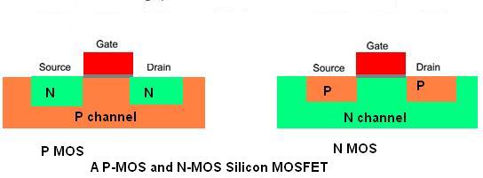
In 1950s, when industry has moved from vacuum-tube diodes and triodes to solid-state diodes and transistors, electronics device researchers have selected Germanium as their semiconductor material. Early solid state diodes and bipolar junction transistors were made using Germanium material. But quickly Germanium replaced with silicon. In today's complementary metal–oxide–semiconductor (CMOS) digital integrated circuits, silicon is used near 100%. Now with the geometries of MOSFET shrinking further down the 14/10 nm, the performance of silicon as MOSFET channel material is questionable, with limitations in frequency of switching, and even the switch itself is erroneously operating. Well the future can be called post-silicon era, where the industry is moving from microelectronics to nanoelectronics/photonics.
IBM said in one of its release "Their (latest Si chips) increasingly small dimensions, now reaching the nanoscale, will prohibit any gains in performance due to the nature of Silicon and the laws of physics. Within a few more generations, classical scaling and shrinkage will no longer yield the sizable benefits of lower power, lower cost and higher speed processors that the industry has become accustomed to." In the immediate future, the transition into <7nm is basically mo...
IBM said in one of its release "Their (latest Si chips) increasingly small dimensions, now reaching the nanoscale, will prohibit any gains in performance due to the nature of Silicon and the laws of physics. Within a few more generations, classical scaling and shrinkage will no longer yield the sizable benefits of lower power, lower cost and higher speed processors that the industry has become accustomed to." In the immediate future, the transition into <7nm is basically mo...
You've read this far — sign in to keep reading