

InGaAs FinFET devices built on CMOS silicon
Sign in to read and print this article.
Imec has announced successful replacement of silicon fins of a CMOS finFET transistor with compound semiconductor material InGaAs fins, so that compound semiconductor (III-V) material based finFETs can be fabricated on a silicon wafer. This achievement helps in volume manufacturability of a chip integrated with both CMOS silicon as well as compound semiconductor material based circuit. By using this process, both RF and logic functions can be integrated in a single monolithic chip, and also can be featured with opto-electronics interface to achieve high-speed data communication both for inter-chip as well as intra chip communication.
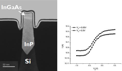
Imec says this achievement leads to manufacturing of high volume heterogeneous CMOS SOC on a 450 MM wafer size. This technology enables manufacturing of hybrid CMOS-RF and CMOS optoelectronics devices at nodes down to 7 nm. This looks like a process where silicon fins were first removed by using some chemical process and then the compound semiconductor is deposited using some advanced atomic deposition process. Imec said its researchers have selectively replaced silicon fins with indium gallium arsenide (InGaAs) and indium phospide (InP), accommodating close to eight percent of atomic lattice mismatch. Imec has used techniques such as aspect-...
Imec says this achievement leads to manufacturing of high volume heterogeneous CMOS SOC on a 450 MM wafer size. This technology enables manufacturing of hybrid CMOS-RF and CMOS optoelectronics devices at nodes down to 7 nm. This looks like a process where silicon fins were first removed by using some chemical process and then the compound semiconductor is deposited using some advanced atomic deposition process. Imec said its researchers have selectively replaced silicon fins with indium gallium arsenide (InGaAs) and indium phospide (InP), accommodating close to eight percent of atomic lattice mismatch. Imec has used techniques such as aspect-...
You've read this far — sign in to keep reading