Digital Lithography Tech for large chiplet based sysmoore kind of Heterogenous large substrate packages
Leading semiconductor equipment maker Applied Materials in partnership with Ushio has announced what it claims has breakthrough Digital lithography technology to manufacture advanced heterogenous integrated 3-D packages by using multiple chiplets. This equipment is basically made to form submicron patterns on large-sized advanced substrates such as glass. This equipment to help manufacture most advanced AI chips for the new era of AI computing.
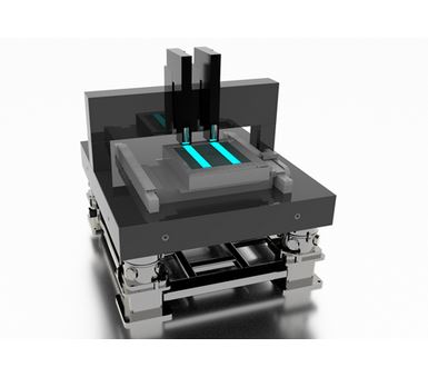
Image Source: Applied With the monolithic scaling becoming tougher and tougher and also very expensive, the semiconductor industry is clearly heading towards heterogenous integrated 3-D packages with already lot of successful products in the market. There is a boom in the market for such products, to address the growing demand semiconductor manufacturers are looking for highly advanced semiconductor lithography equipment to achieve high resolution and also high throughput so that high-volume demand can be met to serve the very fast growing AI chip market. The industry is seeing huge demand for AI chips from companies such as nVidia, where the lead time is significantly high. These advanced equipments can help the leading semiconductor fabs to manufacture s...
Image Source: Applied With the monolithic scaling becoming tougher and tougher and also very expensive, the semiconductor industry is clearly heading towards heterogenous integrated 3-D packages with already lot of successful products in the market. There is a boom in the market for such products, to address the growing demand semiconductor manufacturers are looking for highly advanced semiconductor lithography equipment to achieve high resolution and also high throughput so that high-volume demand can be met to serve the very fast growing AI chip market. The industry is seeing huge demand for AI chips from companies such as nVidia, where the lead time is significantly high. These advanced equipments can help the leading semiconductor fabs to manufacture s...
You've read this far — sign in to keep reading