HomeProductsProducts Details

3D NAND process leveraging 3DX-DRAM offer 28 Gb with 230 layers

Date: 04/05/2023
Finding new solutions to increase the memory density both in flash memory and DRAM is becoming highly challenging. NAND flash could go three-dimensional to achieve high-density. However in today's manufactuing technology 3D multilayer DRAM fabrication can not be made like how 3D NAND flash fabricated.

A new concept in DRAM cell fabrication enable higher density in monolithic DRAM chip using NAND like 3D structure. A company named NEO Semiconductor announced a new three-dimensional 3D X-DRAM. It is a 3D NAND-like DRAM cell array where it provides high densities (up to 8 times higher than the competitors) compared to present DRAM. NEO own 10s of patents on this technology.

3D X-DRAM to use floating body cell technology, where it deviates from using capacitor, a must in present DRAM cells. The structure of the cell is similar to the cell of 3-D NAND flash memory. Due to this it is possible to achieve high density of 128 Gb by using 230 layer structure. It stores electric charges on a floating body without capacitor. NEO claims 8X density and capacity improvements per decade with this technology.

3d -xdram
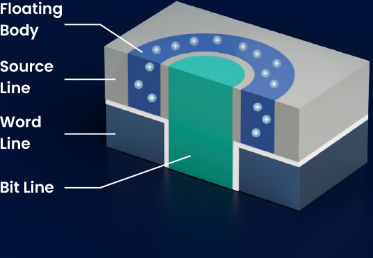
Pic above: 3D X-DRAM cell

3d -xdram
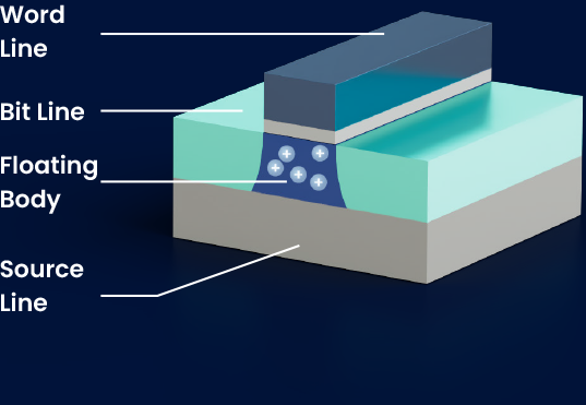
Pic above: 2D Floating Body Cell

3d -xdram
Pic above: 3D X-DRAM Array structure

3D X-DRAM based DRAM chips can be fabricated using present 3D NAND-like process where it only uses single photo mask to define the bit line holes and form the cell structure inside the holes. So the silicon wafer handling process steps are simple and lesser resulting in high-yields.

Andy Hsu, Founder and CEO of NEO Semiconductor claims his company invention, compared to the other solutions in the market is very simple and less expensive to manufacture and scale.

3D X-DRAM uses NAND flash memory wafer manufacturing like facilities and semiconductor equipments to make high density DRAM chips is cost-saving, process saving and equipment saving.

Neo also listed two more technologies it owns in the semiconductor memory domain on its website. They are:
1. X-NAND: By using a new architecture, QLC NAND random read/write speed can be increased by three times and sequential read/write can be improved by 15 to 30 times. Company claims this low-cost solution can be applied to all generations of flash memory such as SLC, MLC, TLC, QLC and PLC.

xnand


2. X-DRAM: Though the company doesn't talk much about this DRAM technology called X-DRAM, the image in the company website's page suggests it is a crosspoint like structure where one sense amplifier connects to four bit lines (BLs) . It takes advantage of longer hold of capacitor charge by lowering the minimum voltage across the capacitor to 0.71V compared to conventional DRAM value of 0.93V. NEO claims X-DRAM offers lower power consumption, lowers latency, and increase throughput.
xdram


Intel wanted to make a single memory device serving both DRAM and flash memory. Intel failed make its technology called 3D Xpoint successful for mass production. Intel promised a lot on this, but could not replace as single memory for both Flash and DRAM. With this NEO technology, there can be a hope that in future a non-volatile memory device can serve either as DRAM or flash.

To learn more visit: https://neosemic.com/3d-x-dram/

To give you some nice social media posts on this:
Fredrick Chen of Winbond asks the question of The diagrams look oversimplified, i.e., potentially wrong. What's with the bit line-word line intersection?
Where there is a response saying "The announced cell structure is just the basic form. The real structure may contain other features. We will disclose more details in hashtag #FMS2023 ."

Access the post at: https://www.linkedin.com/posts/garal-das-aa895417a_neo-semiconductorlaunchesits-ground-breaking-activity-7059806640702668800-f1Cq?utm_source=share&utm_medium=member_desktop

In another post Mark Webb had asked "can we see the mini array results for the 3D DRAM? If we are going to see a 16Gb+ array in production by 2027, then the mini array needs to already be complete and fully characterized per the memory PLC timeline. If it’s a concept with no mini array, then it wont be ready til 2030 at earliest . See timeline details at our website. Www.mkwventures.com"

To which Andy Hsu the CEO of NEO replied "The curve is not a suggested timeline for manufacturing start dates. It is an estimated density of 3D X-DRAM based on the roadmap of the existing 3D NAND technology. The reason of using 3D NAND data as a reference was because 3D X-DRAM manufacturing process is extremely similar with 3D NAND. The 3D X-DRAM density will increase as the number of 3D NAND layers continues to increase over time. The actual density of 3D X-DRAM is dependent on the advancement of 3D NAND process at that time. I will add additional information on the diagram. Hope this clarified. Thank you so much for the comments about PLC timeline on your website. It’s really helpful. Thank you very much!"

Access this post at: https://www.linkedin.com/posts/marcomezger_dram-technology-chip-activity-7060010217232633856-hrZX?utm_source=share&utm_medium=member_desktop