

Direct Cu etch and Co Electroless Deposition for <10 nm IC metal interconnet
Sign in to read and print this article.
Along with the technology challenges of scaling MOSFETs in sub 10 nm IC chip fabrication, there is also challenges involving metal interconnects at deeper nodes. Cu damascene process is used for fabricating copper interconnects. But at deeper nodes, damascene process causes resistivity and reliability issues such as increased grain boundary and surface scattering. Here are the two latest innovation in metal interconnect technology:
1. Researchers at Japanese semiconductor equipment maker Tokyo Electron and Belgium based imec and have found a solution to replace damascene process with a direct Cu etch scheme for patterning Cu interconnects. They have presented a paper at IEEE International Interconnect Technology Conference (IITC) conference on May 18 – 21, 2015 at Grenoble, France.
Tokyo Electron said in its release: When scaling damascene Cu interconnects, reliability issues occur because the overall copper volume is reduced and interfaces become dominant. Direct Cu etch process keep the grain sizes larger and the electromigration performance is preserved by applying an in-situ SiN cap layer that protects the Cu wires from oxidation and serves as the Cu interface, explained by Tokyo Electron.
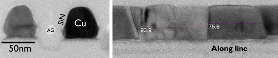
Picture above: TEM section of copper etched lines encapsulated by SiN ...
Picture above: TEM section of copper etched lines encapsulated by SiN ...
You've read this far — sign in to keep reading