By Pratik Damle, Gaurav Mathur, Apurva Sen, Tejinder Kumar, Rajkumar Nagpal, and Rakesh Malik, STMicroelectronics India
Introduction: Product development cycle time is always crucial for any company in any business. In the present era of continuous enhancements in wireless communication, computing, consumer electronics and other similar sectors, silicon providers face lot of challenges to deliver their solutions with quality and on time. To expedite the development cycle, exhaustive and robust automation is gaining high importance in all the phases of product life cycle i.e. design, verification, validation, sustenance. This article presents the architecture of an automated test setup used for validation of mixed signal IPs (Intellectual property) and is demonstrated through high speed serial link PHY (Physical Layers) like USB2.0, MIPI, HDMI etc. and its advantages in terms of massive cycle time reduction and error free tests results. This approach can be used in the validation of any IPs which uses multiple setups for characterization.
CHALLENGES:
The silicon of any high speed serial link PHY is required to be tested and characterized for number of internal blocks and interfaces, over PVT (process, voltage and temperature) variations. To accomplish all these test scenarios, it takes huge amount of time to perform the same test repeatedly on PVT variations, if done manually. Also the validation setup needs to be changed many times while moving from one test case to another. For example in case of a high speed USB transceiver tests, transmitter characterization needs the DUT (device under test) to be connected to scope, while receiver tests are done with data generator connected to the DUT. Similarly Voh, Vol level tests need a digital multi-meter connected at serial interface whereas source meters are used in case of driver current measurement. Also in all the tests some discrete components are required to be connected at serial interface as per test requirement. During the testing, test engineer has to switch across these connections manually as test cases are executed.
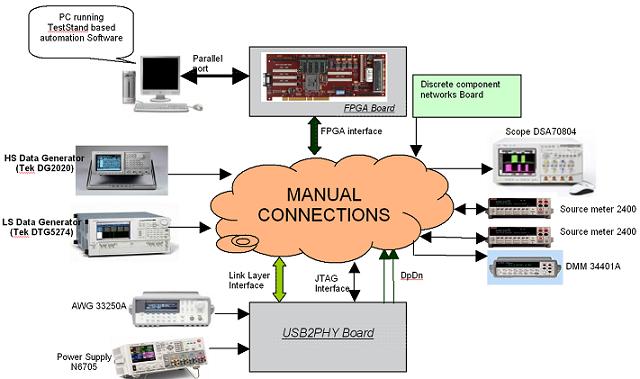
Fig. 1: USB2 PHY test setup
USB2.0 PHY test setup is shown in in figure1. USB2.0 PHY mounted on test board is connected to a number of equipments, components, fixtures, cables at its serial as well as parallel interfaces, which are connected and disconnected to PHY as needed in a particular test.
The iterative execution of tests and setup changes lead to several issues:
- Consume a lot of setup time, which may be more than actual test time.
- Manual mistakes in connections
- Wear and tear of cables, connectors etc due to repeated handling.
- Reliability and repeatability of setup and results.
SOLUTION:
In view of these issues, the development of an automated setup is inevitably gaining importance in industry.
To address the need, an automated test setup was conceived and realized in test Lab using Labview and Test stand as software, customized controller on FPGA Hardware and a complex Switch Matrix board for configurable connections.
All USB2.0 PHY tests are scripted in Labview and integrated in a Test Stand software suite. This software runs on a central controller PC which governs the operation of all equipments in the setup as needed for a test case and ensures error free execution of test cases followed by report generation.
This also controls the customized H/W blocks in FPGA specifically designed to configure the USB PHY for different test cases.
A circuit board as shown in figure 2 is developed, which has a complex switch matrix implemented on it. This board has different ports which make connections with all the equipments, components, fixtures, cables needed in the setup and finally connects them to DUT.
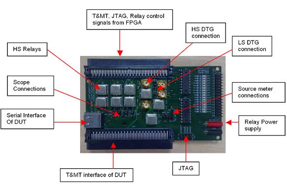
Fig. 2: Switch Matrix Board
The switch matrix is implemented with high performance Teledyne RF relays which can dynamically switch test signals from one port to another while perfectly meeting signal quality requirements. This board is designed so as to ensure the signal quality and path delays conforming to USB interface standards.
The switching of relays is controlled by FPGA which is in turn controlled by Labview script integrated in Test Stand automation suite.
Figure 3 below shows a section of matrix implementation in which different equipments are connected to PHY using relays

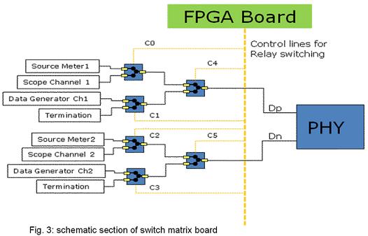
Table below shows the combinations of control lines for connecting different equipments to PHY.
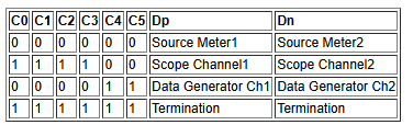
Figure 4 below shows a complete automated setup with the Switch matrix board deployed.
Fig. 4: USB2PHY test setup with switch matrix
Switch matrix methodology is applied in characterization of other IPs also. For e.g. switch matrix is deployed to reduce test time in validation of MIPI D-PHY (Mobile Industry Processor Interface, for 500Mbps) physical layer.
One limitation of switch matrix is that, it distorts the signal as there are of multiple relays present on high speed signal traces which cause signal attenuation and also creates impedance mismatch in signal path. Thus it introduces inaccuracies in test measurements done at high speed signals.
This problem is overcome by compensating the amount of signal degradation imposed by extra circuit in switch matrix in the measurement results. The compensation is used for both Transmit path and receive path. When the board is configured for receiver characterization, the data generators connected to the board are calibrated up till the probe points which negate the signal attenuation and distortion due to the relays present between the probe point and the data generators. For transmitter tests, the degradation is removed by de-embedding the effect of relays and additional traces from the measured signal on the scope. This is done by making a model of the circuit on the board and importing the S-Parameters of the relays into the model.
The effect of de-embedding is seen in the following comparative eye diagrams:
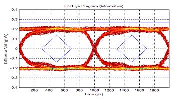
Fig. 5: MIPI D-PHY Transmit eye diagram without switch matrix

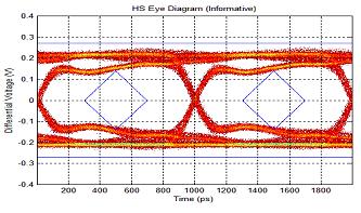
Fig. 6: MIPI D-PHY Transmit eye diagram with switch matrix
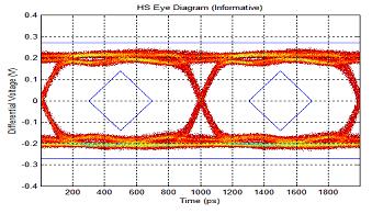
Fig. 7: MIPI D-PHY Transmit eye diagram with switch matrix effects compensated
The eye diagram of the MIPI D-PHY High Speed signal in Figure 5 is plotted using a MIPI D-PHY chip on a board which does not have any relays on the high speed side whereas Figure 6 shows the eye diagram with multiple relays on the high speed side. The degradation of the signal is easily seen. When effects of the relays are removed using the de-embedding technique, eye diagram is improved as can be seen in Figure 7, which is quite comparable to figure5 when there were no relays in high speed data path.
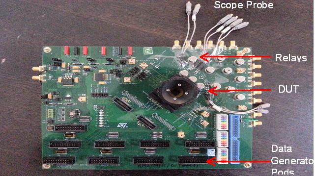
Fig. 8: MIPI D-PHY test board with switch matrix relays
Figure 8 above shows the Switch matrix used for characterization of MIPI PHY with high speed signals. In order to eliminate the effect of PCB to PCB connector the Switching relays are populated on PHY board itself (unlike USB, where switch matrix was implemented on separate board). S- Parameters of relays and related traces are measured and used for de-embedding
SUMMARY:
Thus by deploying switch matrix technique in validation, major gain is achieved in test time. The setup has been successfully deployed for USB2.0 and MIPI D-PHY characterization in Test Lab at ST and offers below remarkable advantages:
- Reduces test cycle time with improved reliability and repeatability of results.
- Prevents any damages to Hardware, equipment due to human error.
- Prevents the degradation in performance of connectors/cables due to repeated connection and removal cycles.
- Makes the test platforms operator-less, thus saves manpower.
Figure 9 below highlights the actual test cycle time reduction achieved in the Lab for USB2.0 PHY. It shows reduction in test time from as setup was matured from "No Automation" to "Complete Automation". As it shows, Test time has been reduced to 2.5 weeks from 14 weeks with an automated setup. It can be further reduced to just 1 week if setup remains operational 24 X 7.
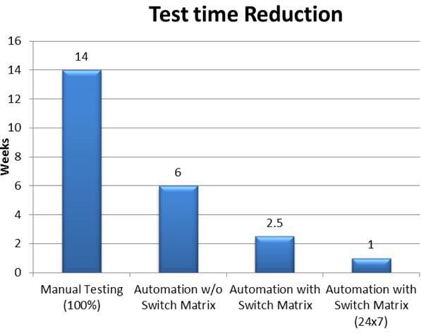
Fig. 9: USB2PHY test time reduction