By Giuseppe Longo and Filippo Scrimizzi, ST Microelectronics
INTRODUCTION
In most applications a power MOSFET works in switching mode. In order to reduce its power dissipation the device switches on to have the minimum voltage drop Vds. Instead, in specific applications power MOSFET devices are used in operating mode called “Linear zone”. The linear zone is that output characteristic area, where the Ids is almost controlled by the Vgs value. In linear mode operation the device is similar to a variable resistor, in which the value is selected by Vgs and by an external voltage power supply and load condition. In this report the technical results performed will be shown at bench in automotive applications which work in linear mode, comparing new trench technology devices with planar ones.
LINEAR MODE OPERATION DESCRIPTION
A power MOSFET device is designed to achieve the best performance in terms of efficiency and reliability in customer applications. The main parameters can be summarized as follows: on state resistance Rdson, threshold voltage Vth, breakdown voltage BVdss, gate charge Qg, reverse recovery parameters and low voltage drop during the operation of body drain diode. Furthermore, the device has to be reliable in terms of:
- Temperature management
- Life time
When the power MOSFET works in linear mode, the main features are limited only to managing temperature and robustness in what is known as thermal instability or thermal runway. The operation in linear mode is characterized in choosing Ids current and Vds voltage drop by a Vgs voltage selected by feedback control driver (almost always the control signal is set to join a specific current value). In this condition, the device power dissipation becomes high and the mean junction temperature increases its value. During this phase the device working stability depends on the intrinsic structure features and exchange heating system.
The temperature is an important factor, since if the max rating is exceeded, the device fails. When the device is at thermal steady state, the current is limited by the temperature because the Rdson increases with it and consequently the current is forced to an auto limitation. However, in linear mode other factors can contribute to bringing the device to exceed the maximum temperature. These factors are:
- Non uniform power dissipation
- Zero tempco point
- Technology features
The power dissipation achieves high values when the device works in linear mode, because the device works with high voltage drop and high current, so that the intrinsic temperature increases rapidly. This means that total junction-ambient Rthj-a thermal resistance (device+heatsink) has to be chosen in a proper way to dissipate the total heat amount in external ambient. Moreover, in the source surface, the areas next to the source wire bonding become hot spots due to the high power management, therefore the local temperature can exceed the max rating.
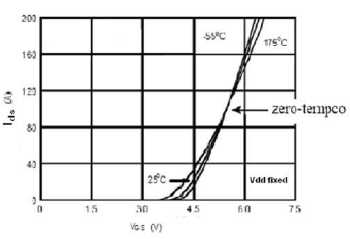
Zero tempco defines a specific feature of the power MOSFET device at a certain temperature. If we trace the curve Ids vs Vgs at various mean junction temperatures, we obtain the following graph:
The curve is traced at fixed Vds values, so that for each Vds value we have a different curve Ids vs Vgs . This curve shows that if the “Vgs>Vgs zero tempco” the current decreases its value if the junction temperature increases. Instead if the Vgs>Vgs zero tempco the current increases if the temperature increases. “Zero tempco” is the temperature matching point of curves Vgs-Ids at a fixed Vds value. If the device is working exactly at “zero tempco” point, the current Ids remains constant at a changing temperature. In our case, the device is working in linear mode at Vds fixed values, the matching point Ids-Vgs can be lower zero tempco and so it works in unstable condition because each temperature increase causes an increase of current. This phenomenon could increase when during the normal working conditions in the application; the Vgs is reduced by the control driver, for a fast reduction of the load. The increasing current for an increasing temperature can determine the thermal runway. The thermal runway is an unstable condition that occurs when the temperature increases without control until the device fails. The phenomenon is emphasized since the power dissipation is high and non uniform power distribution makes hot spots where the temperatures can exceed maximum rating. Even if the device has a well designed heat-sink, the hot spots are difficult to control because the heat-sink helps to reduce its total mean junction temperature not the hot spots that are localized in small areas.
Technology has referred to the procedure and skills to create a device with specific parameters. Designers receive inputs by customer to define a device with the right matching parameters but sometimes to improve the ones they are forced to get others worse. In general, new devices are characterized by two main principal features:
- Low Rdson
- Low Gate Charge, Qg
The two features are joined by specific work processes that allow the achievement of high currents in areas that are always smaller, in order to have high max current, low voltage drop Vds, fast switching. But these features on the other hand, make the device not properly work in linear mode because the high current capability in a small area creates a high current density. So during linear mode operation, hot spots become hotter and consequently the device can probably fall in thermal runway.
Linear mode working is preferred by some automotive customers, and some power devices are designed to operate in this mode. The typical application is VBC (variable blower control) that is the air ventilation system for automotive air conditioning.
The advantages can be summarized as follows:
- The electrical load variation is fluent and linear when device switches from a working point to another one
- The driver circuit is very simple to realize
- Electromagnetic interference are null since the device doesn’t switch
Instead, the drawbacks are:
- High efficient heat-sink need
- High power dissipation device at medium load not recoverable
- Potential thermal runway trigger.
TEST BENCH
In this chapter we'll illustrate the test results performed on VBC, where the main switch, that is a power MOSFET, works in linear mode.
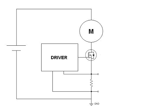
The picture above shows a typical electrical scheme. The power MOSFET working in linear mode, can be assumed like a variable resistor, limiting the motor current and consequently the power dissipation.
On the application system we tested two kinds of devices on bench:
- Planar technology characterized by higher Rdson per die size
- New trench technology with lower Rdson per area.
The application system has the main power device fixed by a screw to a big heat-sink with Rth = 7°C/W, and the heat-sink is inserted in the plenum and ventilated by air flow of motor, which means the equivalent thermal resistance can have lower value that depends on the air flow velocity. The air flow velocity is high at high duty cycle and low at low duty cycle. A thermo resistor control assures that, if the system temperature exceeds a certain value, the control feedback increases the duty cycle at max value to increase the air flow ventilation and so reduces the system temperature.
In the application system the following steps were performed:
- device power monitoring and plastic body temperature measurement at various duty cycles
- device power monitoring and plastic body temperature measurement at various duty cycles with heat-sink not ventilated by air flow, with disconnected control thermo-resistor
- Dynamic switching variation of the duty cycle from 0% to 100%
- Load short circuit test for 30ms
- Load dump by pulse generator
The selected device for this testing was the STP141NF55. During the test at various duty cycles the max plastic body temperature was around 129°C with a power dissipation of 75W in continuous mode. The working operation at various duty cycles was stable, and when the test was finished, the main device parameters were tested, and all measured values were found aligned to the datasheet ones.
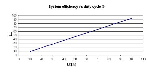
The above picture shows the system efficiency vs. duty cycle. The variation is almost linear and the max efficiency is achieved when the duty cycle d is at maximum value.
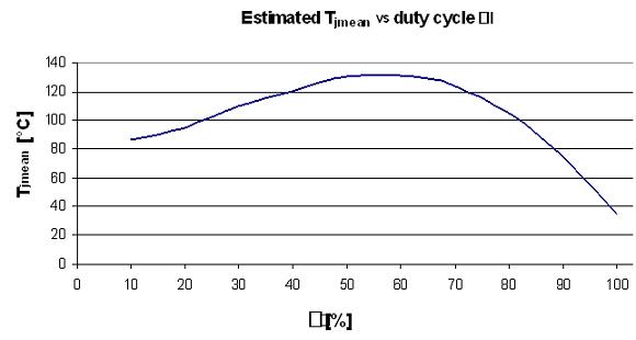
The picture above shows the estimated Tjmean vs duty cycle d. The Tjmean was calculated at thermal steady state at each d, by measuring plastic body and heat-sink - copper frame interface temperature and by the device thermal impedance Rthj-c . The graph gives us a clear idea that the max temperature is joined at around 50%-60% d, that are in general the common working values. At lower and higher d than the above specified value, the temperatures have low values, for the following reasons:
- at low d the power dissipation is low so the mean device temperature is low
- at high d the power dissipation is low since the device works at low Rdson and at the same time the air flow joins the max velocity
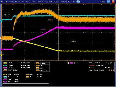
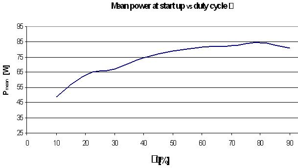
During the test, we also monitored the power dissipation at start up for each duty cycle d, (see the above picture). The power dissipation joins a high value due to the matching of high Ids - Vds. During this start up, we measured the device temperatures and calculated the estimated junction mean temperatures vs. duty cycle d (see the picture below):
The graph shows that the max temperature achieved is around 85°C at 80% d when the device current is almost at max value.
To have a clear estimation of the max power stress allowed on the device involved, we performed a test with the heat-sink out of the plenum and disabling the thermo resistor. The test was performed starting from low duty cycles continuously monitoring the plastic body temperatures. The device failed at 30% duty cycle after almost 25 minutes continuous working, joining in the plastic body case a temperature of 330°C. The result gives us an indication that the device has a high thermal stability before failing. In fact, the thermal runways happened after the plastic body exceeded 330°C. The high temperature managing, in linear mode, is sustainable for devices having low current density per area, to avoid the creation of hot spots that exceed suddenly the max failure temperature of the silicon die.
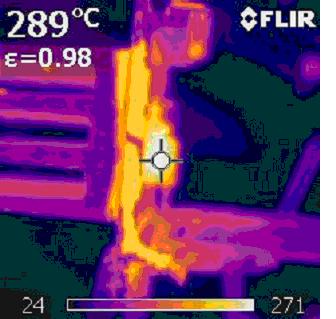
The picture shows a device thermo picture with not ventilated heat-sink/board. In this case the working condition, even if the temperature exceeds the absolute max rating, is still stable. This working condition at this high temperature guarantees the thermal stability of the device.
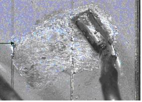
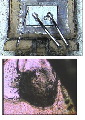
The picture above shows the source surface area of a failed STP141NF55 after chemical opening. It can be noticed that the burnt area includes the area around the source wire bonding pad.
The area that is not uniform is the one where the hot spot is starting, next to the source wire. Since the power density is higher than the boundary limits (the current density increases its value when is next to the source wires), but was a consequence of difficult heat transferring by heat sink. The following tests were also performed on the board:
- Load short circuit test
- Load dump by pulse generator
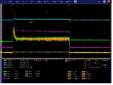
The load short circuit test was performed by a temporized contactor for 30ms
Load dump at 150V 350ms ; the board was working at d = 50%
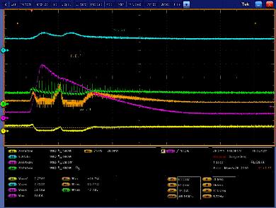
The load dump was also performed by a temporized contactor connected to a power supply. The test was set at 50V-50A for 100ms. This load dump (very stressful) destroyed the device (short all pins). In general, this specific load dump never happens in systems during its working life, but it gives us an estimation of absolute maximum rating (see typical waveform below):
During this load dump the Ids and Vds quickly join high values with high power dissipation peak.
In the application STP141NF55 was replaced by a new trench device and the test results were vice versa negative. The device failed almost instantaneously when the duty cycle was switched on. This confirms that high current density technology makes a device weak in linear mode operation. In fact, linear mode working inside the device structure creates hot spots that probably exceed the 330°C, pushing the device itself in thermal runways.
The test was repeated many times and after that, one sample was chemically opened and analyzed by microscope. The picture shows the details of the failures:
The black area next to the right source wire is the area where the hot spot begins exceeding the max silicon temperature. The failure point probably is due to the bonding source wires, which are the areas where there is max current density. The boundary of the black area is well defined, meaning that the hot spot starts very rapidly fusing the silicon without spreading to other areas.
The hot spot are smaller areas that are characterized by high temperature because the current density is high. So statistically the thermal runway has more probability to start in this area than other ones.
Conclusions
The SP ST MOSFET technology is suitable for linear mode applications where not only the power dissipation capability is very important, but also the thermal instability robustness. Vice versa the new Trench power MOSFETs have an even higher equivalent cell density per area and then a lower Rdson. These Power MOSFETs do not work properly in this kind of application because of their intrinsic weakness linked to the thermal runaway.