While Moore's Law states that the number of transistors that can fit on an integrated circuit should double every two years, this is getting harder and harder to achieve, as transistors reach atomic dimensions. One of the biggest problems is the way power dissipation increases as more transistors are added. But the researchers have come up with an entirely new logic circuit family based on magnetic semiconductor devices.
Unlike traditional integrated circuits, which consist of a collection of miniature transistors operating on a single piece of semiconductor, these 'spin logic circuits' exploit the quantum physics phenomenon of spin, another fundamental property of the electron in addition to charge property.
The device called Quantum Dot which houses a single electron can be configured in a logic circuit that is capable of performing all the necessary Boolean logic and can be cascaded to develop sophisticated function units. These 'spintronic' logic devices successfully perform the same operations as a conventional CMOS circuits, but with fewer devices and more computing power.
Conventional charge based Logic Design result in enormous power dissipation since information is stored at two different charge levels. Charge being a scalar has only magnitude. So logic levels can solely be defined only by presence or absence of charge. In order to charge or discharge capacitor to define logic 0 or logic 1 current has to flow which result in power dissipation. However we can use spin degree of freedom of an electron to define the logic. Spin being a vector, electron has fixed magnitude but can be polarized in any direction to get bistability. A single electron in a Quantum well can be oriented to have either UP spin or DOWN spin with external magnetic field to define logic 0 or logic 1.Switching can be done just by flipping the direction without actually causing the motion of the charge. This results in considerable saving of energy.
However there is still power dissipation involved in flipping the Spin which is gµB, where B is the global magnetic field which is required to maintain spin polarization bistable, g is the Lande g factor and µ is the Bohr Magneton . The external field required to orient electron spin depends on acceptable error probability in the Logic Design. Magnetic Field “B” can be made extremely small to reduce power dissipation. However this results in frequent flipping of Spin resulting in error. In order to encode bits reliably spin polarization should not flip frequently. This is important because we cannot refresh spin bits frequently as it results in power dissipation. Hence it is required that the Spin relaxation be long enough. If the electron polarized in particular direction is housed in a Quantum Dot the relaxation time in quiet high. Because of weak spin orbit interaction Quantum Dots are generally fabricated with InP or GaAs.
Universal Logic Gate Design with Single Spin
We can realize any logic gate or entire combinational circuit with two dimensional array of Quantum Dots containing single electron. The Quantum Dots interact through nearest neighbor exchange interaction. Through nearest neighbor interaction what we understand is that the wave function of electron in one Quantum Dot overlap with the wave function of electron only in its nearest neighbor Quantum Dot. Certain Quantum Dots in the array are defined as input ports and the spins of the electrons in these input ports are defined by local Magnetic Field. Nearest neighbor interactions and the states of input spins determine the spin state of other Quantum Dots in the array. By properly arranging Quantum Dots in two dimensional array we can ensure that the output takes the values determined by the Truth Table for the logic gate being implemented. We show below implementation of Universal NAND gate with Quantum Dots.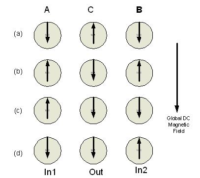
Fig.1.Nand Gate Implementation with Quantum Dots
As shown in the figure above NAND gate can be implemented with three Quantum Dots.Dots A and B define input port and Quantum Dot C between A and B define the output. Global Magnetic Field B determine the Quantization Axis for the Spin i.e. Spin in any Dot may be either parallel or Antiparallel to this. Parallel is defined as logic 1 and Antiparallel state is defined as logic 0.As defined earlier only nearest neighbor interactions are strong.If we apply logic inputs to Dot A and B and allow the system to relax to thermodynamic ground state the logic output in Dot C is always conforms to the truth table of NAND operation of Inputs A and B.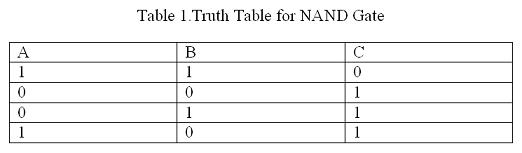
Once we have NAND gate any arbitrary circuit can be implemented. One severe drawback with this design is unidirectionality in time is not possible since exchange interaction is bidirectional. So Clock pads which are not shown in the above figure are used to raise or lower the barrier height between the Dots. If the barrier height is increased by applying voltage at the clock pad then there is no wavefunction overlap and hence the Dots are isolated.If the barrier is lowered again by applying voltage at the clock pad then the overlap of wavefunctions take place through exchange interaction. Hence Unidirectionality is ensured.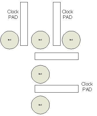
Fig.2. Quantum Dots with Clock PADS to control the barrier height
How to read and write Single Spin
The next issue is how to align spin of electron housed in Quantum Dot to define Logic 0 or Logic 1.This is done by local magnetic fields generated by inductors which will orient the spin parrel to the field and hence write the logic. Reading the bit information from the output is slightly complex and is generally done by highly precise magnetic resonance force microscopy.
Major recent advancements in manipulating single spin of an electron in Quantum Dot has made it possible to realize Ultra Low Power Logic Gates. Practical implementation may take some time but Spintronics will surely replace traditional Silicon Based Electronics in some near future.