Triangle of collaboration for finFET success
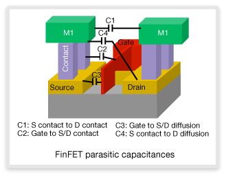
The semiconductor industry is moving towards 3-D FinFETs more for performance rather than cost. There is going to be significant drop in leakage current. 14nm FinFET transistors are expected to increase speed performance by 20% and power consumption reduction by 35% and 15% save in space compared to 20nm planar technology. However 3D FinFET's inter-device and inter-connect behavior is not simple mathematics. The capacitance parameters of 3D FinFET is lot more complex compared to 2D.
For the production success of FinFET based 16nm SoCs, the semiconductor foundries, semiconductor equipment suppliers and EDA tool vendors are working extremely closely so that their systems work smoothly across. 14/16 nm FinFET based test chips are already out, the volume production is expected to happen any time in 2014. At the backend, the chip manufacturing technology is getting extremely complex, so much that, it is becoming increasingly difficult to scale any further by using litho techniques. However for a VLSI design engineer, the front-end looks pretty much the same, except that the design flow/process undergoing some changes. There is a lot more automation and design checks to ensure first-time successful tape out. FinFET and double patterning results in a lot of extraction. VLSI d...
For the production success of FinFET based 16nm SoCs, the semiconductor foundries, semiconductor equipment suppliers and EDA tool vendors are working extremely closely so that their systems work smoothly across. 14/16 nm FinFET based test chips are already out, the volume production is expected to happen any time in 2014. At the backend, the chip manufacturing technology is getting extremely complex, so much that, it is becoming increasingly difficult to scale any further by using litho techniques. However for a VLSI design engineer, the front-end looks pretty much the same, except that the design flow/process undergoing some changes. There is a lot more automation and design checks to ensure first-time successful tape out. FinFET and double patterning results in a lot of extraction. VLSI d...
You've read this far — sign in to keep reading