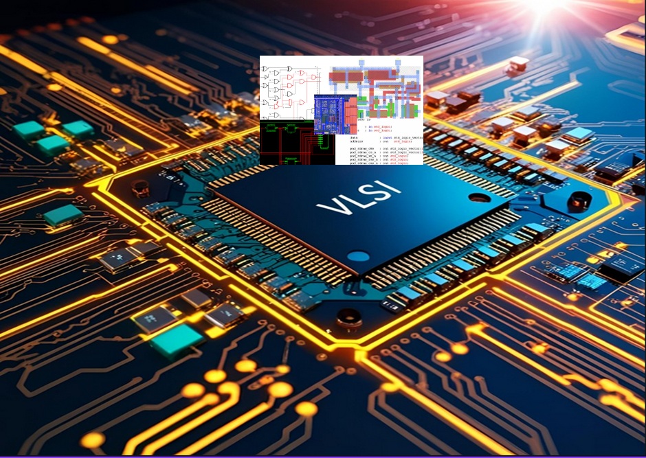
This module covers the fundamental ideas underlying design of modern digital systems. This module explains the basis of circuit elements, how they are interconnected to form digital circuits and also the non-ideal effects of the design. Digital Systems The word digital refers to representing any information in just two voltage levels [logic zero (0) or logic high (1)]. Logic Zero means zero voltage, logic high means some level of electric potential voltage, which is generally a 3.3V or a 5V. Digital systems are more in use than analog systems for processing data due to the following reasons:Digital systems are easier to design as digital system use digital signals which provides many futures such as being very less prone to noise, signal can be easily regenerated etc. The term design reference to the systematic process of working out how to construct circuits that meet given requirements while satisfying constraints on cost, performance, power consumption, size, height and other properties. Let's start discussing about logic gates that operate on digital signal. There are three basic gates namely AND, NOT, OR from this NAND, NOR, XOR, X-NOR gates are derived. NAND and NOR gates are usually referred as universal gates. Now let's start discussing about how this gates work. NOT gate: In a computer world, the character used to represent NOT gate is "~" (or) (!)(negation). When any logic high signal enters NOT gate, output of not will be a low signal and reverse operation takes place when low signal is entering the NOT gate. The symbol of NOT gate is depicted in the figure 1 and its working is represented in truth table. 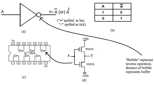
Figure1: (a) inverter symbol (b) truth table © IC for not gate (d) schematic of inverter IC 7404 is used for NOT gate, six NOT gates are embedded in IC 7404. The schematic diagram for NOT gate is illustrated in the figure1 AND gate Unlike NOT gate, AND gate has two input terminals. The character to represent AND function is "& ". Output of AND gate will be high only when both the inputs are high. Symbol for AND gate is as shown in the figure 2 below. 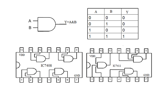
Figure 2: AND gate, truth table and inner view of IC7408 and IC7411 IC 7408 is used for AND operation. It contains 4 AND gates each having two inputs. We can have 3 input AND gate (IC7411). Pin Configuration of IC 7408 & 7411 is shown in the figure 2. We can derive 4 input AND gate by two input AND gate. Let us see how we can do that 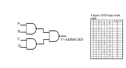
Figure3: 4 input AND gate derived from two input AND gate and its truth . The figure below shows the schematic (circuit diagram) of two input AND gate is made using MOSFETs. 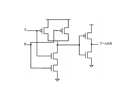
OR gate: Character to represent or gate is "|". OR gate performs addition. When any one input of OR gate is logic high, output will be high. The Symbol and truth table of OR gate is shown in the figure 5. IC 7432 is used for OR operation. It contains four, 2 input OR gates. 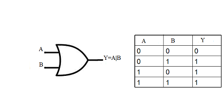
Figure 5: symbol and truth table of OR gate. 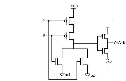
Figure6: schematic of OR gate Note: To learn more on IC numbers for digital circuits visit: https://en.wikipedia.org/wiki/List_of_7400_series_integrated_circuits Switch on the light in a room when the room is dark using a simple AND gate : Here is a real-world example that is always simple, AND gate can be used to switch on the light in a room when the room is dark. Please see the figure 7. It said two input AND gate where one input is connected to a switch which is either connected to +5 V of high-voltage or grounded to 0 voltage. To make this device working you have to keep the switch in such a way that it's connected to +5 V so that the input to the AND gate is always high. The other input up AND gate is connected to a light sensor which produces +5 V whenever there is darkness or no light otherwise zero voltage that is low-level whenever there is light. The AND gate is connected to a relay which can switch on a light bulb. The light bulb will switch on only when both and inputs are high. That is a case only when there is a dark. 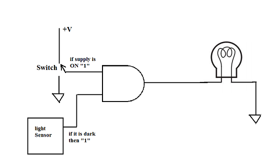
Figure 7: real world example using AND gate. Applications are as simple as this, logic gates controls today's world in the form of complex processor chips which have millions of such gates. In this course, we will take you through how so many millions of logic gates or wired to perform a complex function for real-time usage. We started with logic gates basically to explain with the above application where logic circuits can be used to automate many of our needs. Example 2 Consider a plastic manufacturing plant. Plant should be maintained below with certain temperature and pressure threshold. If temperature or pressure exceeds the limit, the plant should shut down. 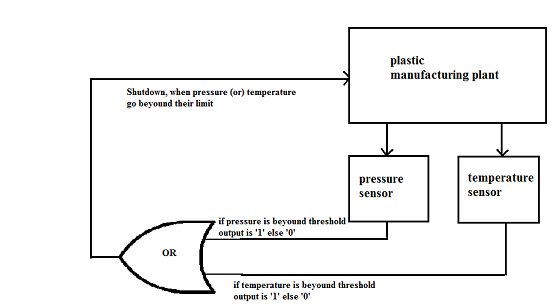
Figure8: real world example for OR gate Example 3 In a real-world inverters of connected back-to-back with odd numbers, then feedback is given from output to input to get oscillation. 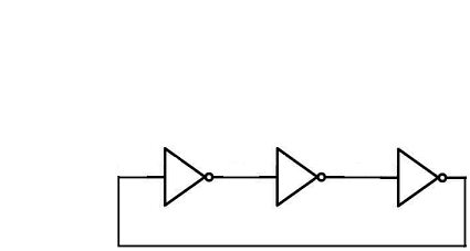
Figure 9: ring oscillator Note: Design should satisfy “Barkhausen Criteria ” refer digital and mixed mode VLSI by Razavi. Universal Gates (NAND and NOR) NAND gate is inverse of AND gate. Symbol for NAND gate is shown in the figure 10. Working of AND gate is explained in the truth table . 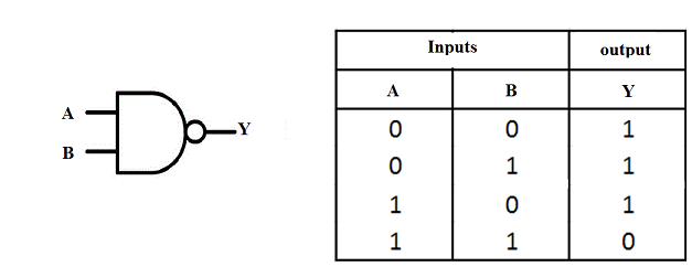
Figure10: symbol of NAND gate and its truth table NOR gate is inverse of OR gate. Symbol for NOR gate is depicted in figure 11. Working of NOR gate is it explained in the truth table 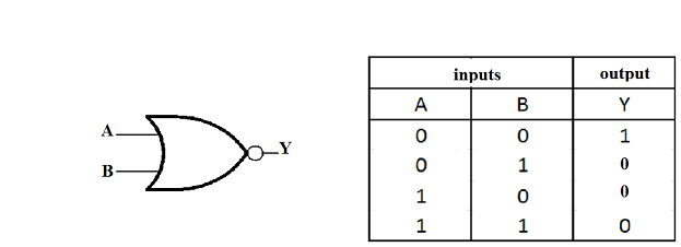
Figure 11: symbol of NOR gate and its truth table From NAND and NOR gate, We can derive any other gates, hence the name universal gates. Let’s see how is it made: NAND as AND gate 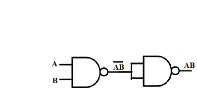
NAND as OR gate 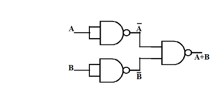
NOR as AND gate 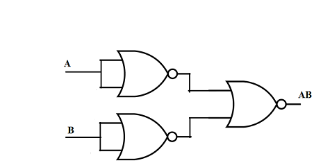
XOR gate: Pronounced as Exclusive OR gate: XOR gate performs module sum operation which does not include Carry. It contains two inputs and one output. The symbol of XOR gate is shown in the figure 12. 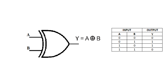
Figure 12: symbol of XOR gate and its truth table NAND as XOR gate 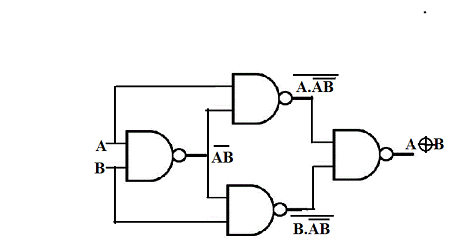
XNOR ( Sometimes referred as EX NOR, ENOR, NXOR) XNOR performs inverse operations on XOR 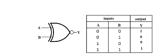
Use of universal gates in real world. Example 1: Consider a scenario Industrial chemicals are stored in warehouses where chemical reactions takes place leading to the production of toxic fumes that are dispensed into atmosphere through exhaust fans. Three exhaust fans have to be implemented in warehouses so as to exhaust poisonous air in the course of its operation. If any one or more exhaust fans fails then an alarm gets activated. 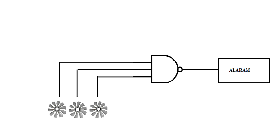
A NAND gate based Exhaust fan failure detection system. Example 2: Washing machine has three sensors to check its operation. The first operation is the functioning of the door while the second is the water level and the third is the weighing of the clothes. If one of the functions fails such as opening or closing of the door, variation in the water level or the overload of clothes, generates appropriate sensor outputs to 1. The outputs of 3 sensors are connected to 3 inputs NOR gate. Sensors outputs will be ‘0’ during the normal operation of the washing machine. The NOR gate output is 0, if an erroneous condition is detected by any one or more sensors.. The NOR gate output is connected to a switch of the washing machine. 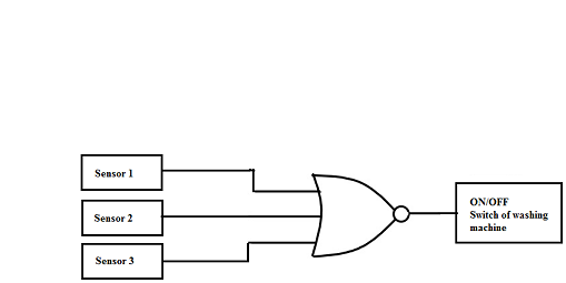
Boolean algebra A Boolean algebra is used as a foundation for digital design. Digital systems can be expressed in terms of Boolean expression which contains Boolean operators, variable and Boolean values. Boolean algebra deals with Boolean expression Example of Boolean expression 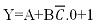
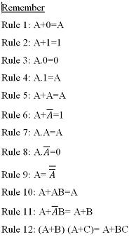
In the example above A, B, C are variables , ‘+’& ‘.’ are operators and ‘0’ & ‘1’ are Boolean values. The axioms for Boolean algebra is listed below: Identity laws X+0=X X.1=X Association laws (X+Y)+Z= X+(Y+Z) (X.Y).Z=X(Y.Z) Commutation laws X+Y=Y+X X.Y= Y.X Distribution laws X+ (Y.Z)= (X+Y).(X+Z) X.(Y+Z)= (X.Y)+(X.Z) Complement laws 
some of the useful theorems are listed below which can be used while dealing with Boolean expressions. Idempotence laws X+X= X X.X=X Absorption Laws X+(X.Y)=X X.(X+Y)=X Further identity laws X+1=1 X.0=0 De Morgans Laws 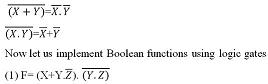
Here ‘+’ represents OR Operation ‘.’ represents multiplication i.e. AND Operation 
(2) f= AB+A(B+C)+B(B+C) 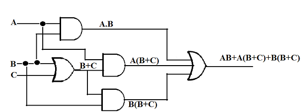
(3) f=A(B+CD) 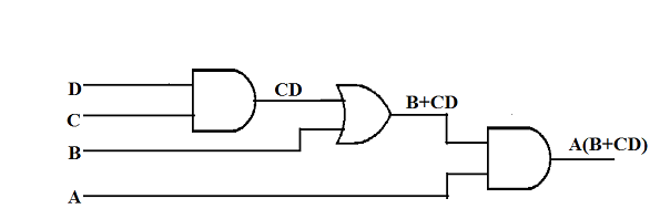
Boolean expressions can be expressed in two forms namely sum of products (SOP) and product of sums (POS): Sum of Products:- Product terms of Boolean Expressions are summed together by Boolean addition to form SOP Example:- 1. AB+BC+CA 2. AB+B(C+D) Product of sum: sum of the variables are multiplied with sum of other terms of the expression. • 
• (A+B+C)A (D+F) We cannot convert Boolean expression into SOP or POS. Let us see how we can achieve it: • AB+B(CD+EF) converted to SOP Ans. AB+BCD+BEF • (A+B) (B+C+D) convert to SOP Ans. AB+AC+AD 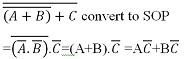
Note:- So for we have seen SOP and POS expressions. There are the examples of non-standard way of expressing Boolean expressions. Standard SOP: Consider an example f= AB+BC+CA, let us convert it to standard SOP form: >AB+BC+CA 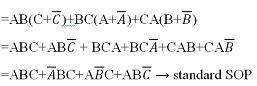
A Standard SOP expression is one in which all the variables in the domain appear in each product term in the expression. Standard POS 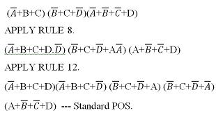
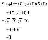
Simplification of Boolean expressions using Boolean algebra • AB+A(B+C)+B(B+C) =AB+AB+AC+BB+BC = AB+AC+BC+B = B+ AC+AB = B (1+A)+AC =B+AC • 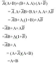
 Simplifying the Boolean expression will simplifies the logic. Consider the expression AB+A(B+C)+B(B+C), it is equivalent logic circuits and simplified circuit diagram is shown below
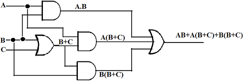
Simplified logic 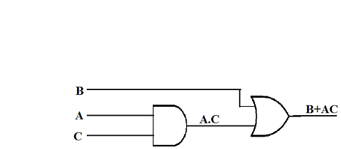
Logic simplification can be done by many methods and some of them are listed below Karnaugh map Quine Mccluskey algorithm State variable minimization For more information about logic simplification go through “digital logic applications and designs” by John M Yarbrough. Non ideal effects of circuit elements (1) Propagation delay: Propagation delay is due to internal switching activity (i.e. the time taken for charging and discharging nature of parasitic capacitance of transistors) The signal levels do not change instantaneously due to switching activity. The time taken for the signal voltage to rise from low-level to high-level is known as rise time. The time taken for the signal voltage to fall from high-level to low-level is known as fall time. 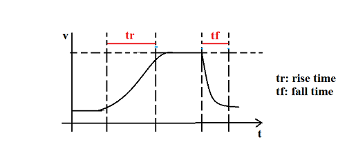
Consider a circuit shown in the figure below 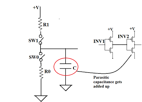
One way to reduce propagation delay is to reduce parasitic capacitance, if more than one logic block is connected to the output of previous block, Parasitic Capacitance gets added up which results to more propagation delay in other words fanout should be less. (2)Wire delay We think that wire acts like a pew conductor without any resistance, but in reality wires will have resistance inductance and capacitance. When wire length is too small these values are very negligible. When wire length is too large, they become a transmission line which has reasonable propagation delay. While designing high-speed systems these delays should be taken into considerations. (3)Glitches Glitches are also known as invalid output which is due to the propagation delay in the inputs entering logic block for example assume a circuit diagram shown below 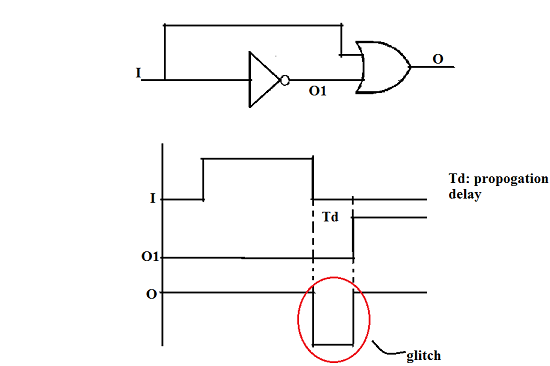
In the above example we can say that unexpected zero at the output of the circuit. This is termed as glitch and it causes problems for the rest of the circuits as it will propagate into the next circuits and results to more glitches. Solution for this problem: adding buffer to the path which has less propagation delays. These buffers compensates the delay so that we can expect correct results at the output. 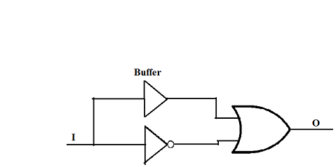
Combinational logic circuits and sequential logic circuits combinational logic circuits performs the operation on the inputs entering the circuit and it determine output as a Boolean function of input. In other words output is a function of input alone. Figure below shows general block diagram of combinational circuit. 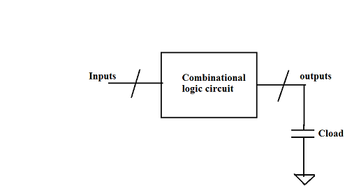
These combinational logic circuits lacks behind in storing any previous outputs. In other words it has no memory. This can be overcome by using sequential circuits, in which output is determined by both previous and present inputs. Figure below shows a block diagram of sequential logic circuits. 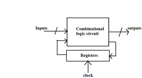
For more information about sequential logic circuits and combinational logic circuits, please refer CMOS Digital integrated circuits by sung mo kang Yusuf leblebic. Digital circuits are classified into synchronous circuits and asynchronous circuits . In synchronous circuits, there will be one global clocks signal that’ll will be driving entire circuits. Advantages of synchronous circuits • Design is simpler • likelihood of correct operation is higher disadvantages routing becomes a problem 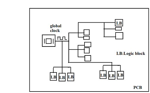
In asynchronous circuits there will be two are more clocks, but they are ideal and synchronous. 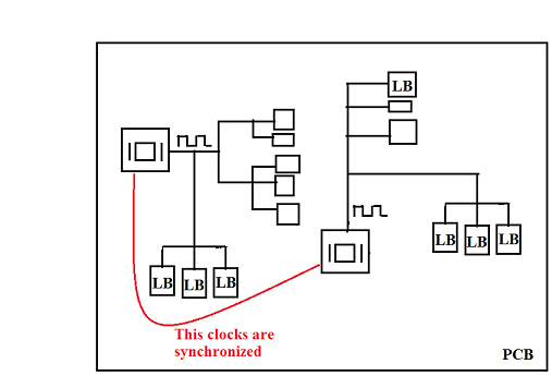
Note:Most of the commercial digital design use synchronous circuits