Keypad/keyboard interface to LPCXpresso
This module explains how to use 4x3 membrane keypad with NXP's LPCXpresso microcontroller board
Requirements:
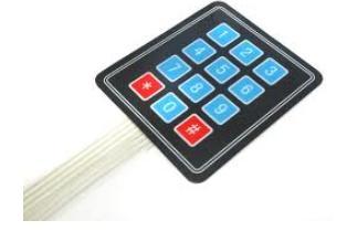
1. 4x3 Membrane Keypad
2. Seven segment display & 3K3 ohms resistors
3. Connecting wires.
4. General purpose printed circuit board.
Keypad is an array of switches. Matrix keypads are very common input devices in embedded systems. They have simple architecture and are easy to interface. One good thing about them is that they allow you to interface a large number of input keys to a microcontroller with minimum usage of I/O resources. This tutorial type module explains how to read input data from a 3×4 (12 keys) matrix keypad interfaced to a ARM Cotex M0 based LPCXpresso microcontroller embedded board from NXP Semiconductor and display the data on a seven segment display. In short this project is to display the pressed key symbol on the seven segment display.
Working: There will be 2 wires connected to each switch of the keypad, they get short circuited whenever a button is pressed. For example; when button '1' is pressed, pin P0.7 and pin P3.2 are connected (as shown in the picture below). Normally when no switch is pressed there is no connection between rows and columns. Whenever a button is pressed contact is made between particular row and column. 4x3 Keypad pins can be directly connected to microcontroller i/o port of this board.
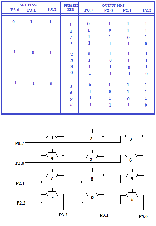
Figures above : Keypad logic table and keypad's row and column pins
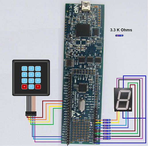
Keypad Interfacing circuit: The below circuit connects 4x3 Membrane Keypad with port 3 and port 2 and port 0 of microcontroller. The 7-seg display is connected to port 2 and port 3 of microcontroller.
Programming :The sample C-program/code below displays coresponding numbers pressed on the keypad . The text below in red color-font is the sample code which you can directly use in your compiler:
#include "driver_config.h" //for including the header file
#include "target_config.h"
#include "gpio.h"

void delay()//delay function
{
int a;
for(a=0;a<30000;a++);
}
void display(int a)
{
LPC_GPIO2->DIR=0x7C8;
LPC_GPIO3->DIR=0x030;
switch(a)
{
case 0:
// for 0
LPC_GPIO2->DATA=0x388;// (set the P2 bits as 0011 1000 1000)
LPC_GPIO3->DATA=0x030;// (set the P3 bits as 0000 0011 0000)
delay();// delay function calling
break;
case 1:
// for 1
LPC_GPIO2->DATA=0x080;// (set the P2 bits as 0000 1000 0000)
LPC_GPIO3->DATA=0x020;// (set the P3 bits as 0000 0010 0000)
delay();// delay function
break;
case 2:
// for 2
LPC_GPIO2->DATA=0x588; //(set the P2 bits as 0101 1000 1000)
LPC_GPIO3->DATA=0x010; //(set the P3 bits as 0000 0001 0000)
delay();// delay function
break;
case 3:
// for 3
LPC_GPIO2->DATA=0x580; //(set the P2 bits as 0101 1000 0000)
LPC_GPIO3->DATA=0x030; //(set the P3 bits as 0000 0011 0000)
delay();// delay function
break;
case 4:
//for 4
LPC_GPIO2->DATA=0x680; //(set the P2 bits as 0110 1000 0000)
LPC_GPIO3->DATA=0x020; //(set the P3 bits as 0000 0010 0000)
delay();// delay function
break;
case 5:
//for 5
LPC_GPIO2->DATA=0x700; //(set the P2 bits as 0111 0000 0000)
LPC_GPIO3->DATA=0x030; //(set the P3 bits as 0000 0011 0000)
delay();// delay function
break;
case 6:
//for 6
LPC_GPIO2->DATA=0x708; //(set the P2 bits as 0111 0000 1000)
LPC_GPIO3->DATA=0x030; //(set the P3 bits as 0000 0011 0000)
delay();// delay function
break;
case 7:
//for 7
LPC_GPIO2->DATA=0x180; //(set the P2 bits as 0001 1000 0000)
LPC_GPIO3->DATA=0x020; //(set the P3 bits as 0000 0010 0000)
delay();// delay function
break;
case 8:
//for 8
LPC_GPIO2->DATA=0x788; //(set the P2 bits as 0111 1000 1000)
LPC_GPIO3->DATA=0x030; //(set the P3 bits as 0000 0011 0000)
delay();// delay function
break;
case 9:
//for 9
LPC_GPIO2->DATA=0x780; //(set the P2 bits as 0111 1000 0000)
LPC_GPIO3->DATA=0x030; //(set the P3 bits as 0000 0011 0000)
delay();// delay function
break;
case 10:
//for *
LPC_GPIO2->DATA=0x780; //(set the P2 bits as 0111 1000 1000)
LPC_GPIO3->DATA=0x000; //(set the P3 bits as 0000 0011 0000)
delay();// delay function
break;
case 11:
//for #
LPC_GPIO2->DATA=0x408; //(set the P2 bits as 0111 1000 0000)
LPC_GPIO3->DATA=0x030; //(set the P3 bits as 0000 0011 0000)
delay();// delay function
}
return ;
}
int main ()
{
while(1)//Infinite loop
{
uint32_t regVal;
/* Use port0_7 as input event, interrupt test . */
GPIOSetDir (PORT0, 7, 0);
/* Port2_1, single trigger, active low. */
GPIOSetInterrupt (PORT0, 7, 1, 0, 0);
GPIOIntEnable (PORT0, 7);
GPIOIntStatus(0,7);
/* Use port2_0 as input event, interrupt test . */
GPIOSetDir (PORT2, 0, 0);
GPIOSetInterrupt (PORT2, 0, 1, 0, 0);
GPIOIntEnable (PORT2, 0);
GPIOIntStatus(2,0);
/* Use port2_1 as input event, interrupt test . */
GPIOSetDir (PORT2, 1, 0);
GPIOSetInterrupt (PORT2, 1, 1, 0, 0);
GPIOIntEnable (PORT2, 1);
GPIOIntStatus(2,1);
/* Use port2_2 as input event, interrupt test . */
GPIOSetDir (PORT2, 2, 0);
GPIOSetInterrupt (PORT2, 2, 1, 0, 0);
GPIOIntEnable (PORT2, 2);
GPIOIntStatus(2,2);
GPIOSetDir (PORT3, 0, 1);
GPIOSetValue(PORT3,0,0);
GPIOSetDir (PORT3, 1, 1);
GPIOSetValue(PORT3,1,1);
GPIOSetDir (PORT3, 2, 1);
GPIOSetValue(PORT3,2,1);
{
regVal = GPIOIntStatus( PORT0, 7 );
if ( regVal )
display(1);
regVal = GPIOIntStatus( PORT2, 0 );
if ( regVal )
display(4);
regVal = GPIOIntStatus( PORT2, 1 );
if ( regVal )
display(7);
regVal = GPIOIntStatus( PORT2, 2);
if ( regVal )
display(10);
}
GPIOSetDir (PORT3, 0, 1);
GPIOSetValue(PORT3,0,1);
GPIOSetDir (PORT3, 1, 1);
GPIOSetValue(PORT3,1,0);
GPIOSetDir (PORT3, 2, 1);
GPIOSetValue(PORT3,2,1);
{
regVal = GPIOIntStatus( PORT0, 7 );
if ( regVal )
display(2);

regVal = GPIOIntStatus( PORT2, 0 );
if ( regVal )
display(5);
regVal = GPIOIntStatus( PORT2, 1 );
if ( regVal )
display(8);
regVal = GPIOIntStatus( PORT2, 2);
if ( regVal )
display(0);
}
GPIOSetDir (PORT3, 0, 1);
GPIOSetValue(PORT3,0,1);
GPIOSetDir (PORT3, 1, 1);
GPIOSetValue(PORT3,1,1);
GPIOSetDir (PORT3, 2, 1);
GPIOSetValue(PORT3,2,0);
{
regVal = GPIOIntStatus( PORT0, 7 );
if ( regVal )
display(3);
regVal = GPIOIntStatus( PORT2, 0 );
if ( regVal )
display(6);
regVal = GPIOIntStatus( PORT2, 1);
if ( regVal )
display(9);
regVal = GPIOIntStatus( PORT2, 2);
if ( regVal )
display(11);
}
}//paramesh
return 0;
}
Click below to visit next and other embedded system course modules
Module 7: Serial communication concepts -1
Module 9: Controller Area Networking (CAN)
Module15: SRAM memory interface
Module16: Flash memory interface
Module17: LCD display panel interface
Module18: Touch pane interface
Previous Modules
Module 1: Introduction to Embedded Systems: Definition, application and future.
Module 2: Microprocessor, Microcontroller, MCU Manufacturers, introduction to programming.
Module 3a: Installation of ARM Cortex M0 based LPCXpresso kit from NXP and sample code
Module 4a: Sample program for LPCXpresso
Module 3b: Installation of ARM Cortex M0 based STM32F0 Discovery kit from ST Microelectronics and sample code
Module 4b: Sample program for STM32F0 Discovery